Wireless Infrastructure
Meeting the continually evolving demands for 4G LTE & 5G wireless infrastructure applications with RFHIC's gallium nitride (GaN) on silicon carbide (SiC) technology solutions


The fabrication of semiconductor devices involves essential processes like deposition, removal, patterning, and electrical property modification. As the semiconductor industry evolves, the demand for smaller, faster, and more efficient devices continues to rise. Challenges such as ultra-thin layers, smaller critical dimensions, innovative materials, and 3D structures require cutting-edge solutions to boost yield and productivity. RFHIC’s GaN solid-state microwave technologies and solutions are designed to help you meet these growing industry demands while maximizing efficiency and performance.
Plasma Technology in Semiconductor Manufacturing
Plasma is often referred to as the fourth state of matter, distinct from solids, liquids, and gases. It is an ionized gas containing free electrons, ions, and neutral particles. Plasmas are essential in semiconductor manufacturing, particularly for etching, deposition, and cleaning processes. By utilizing plasma, manufacturers can precisely control material deposition and removal on the nanometer scale.

What is Plasma?
Plasma is created when a gas is energized by an external energy source, causing some of its electrons to become free from their atomic or molecular bonds. This process generates ions and electrons, forming an electrically conductive medium.
Plasma is characterized by:
Plasma Sources
In semiconductor manufacturing, plasma sources are used in processes like plasma-enhanced chemical vapor deposition (PECVD) and reactive ion etching (RIE). Common plasma sources include:
Plasma Generation Energy Sources
Energy sources such as microwaves, radio frequency (RF), and DC power are used to generate plasma in semiconductor manufacturing. These sources can efficiently ionize gas molecules, enabling precise control over the deposition or etching of materials.
Plasma’s ability to achieve precise material modifications with high energy efficiency makes it essential in various semiconductor fabrication steps.
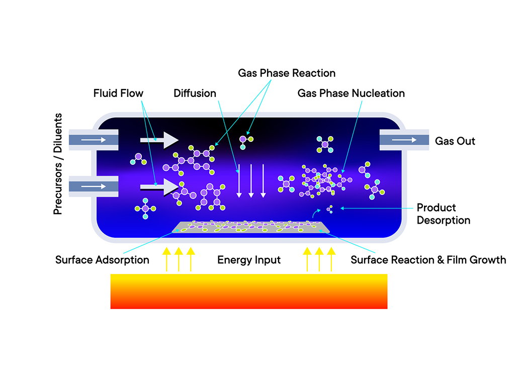
Deposition Technologies
Deposition processes form the backbone of semiconductor manufacturing, enabling the creation of essential layers for transistors, interconnects, and other components. Here are the major deposition technologies used today.
Chemical Vapor Deposition (CVD)
CVD is a deposition process that involves chemical reactions between precursor gases to form solid materials on the wafer. It is widely used to deposit insulating, conductive, or semiconductive layers with high uniformity and excellent step coverage.
Molecular Vapor Deposition (MVD)
Molecular Vapor Deposition (MVD) offers atomic-level precision over film thickness and composition, making it ideal for the deposition of ultra-thin, conformal films under low-pressure conditions. This method is particularly beneficial for nanoscale architectures like MEMS (Micro-Electro-Mechanical Systems) devices, where MVD is used to deposit functionalized organic molecules that modify surface properties.
MVD thin films serve a variety of functions, including hydrophobic, hydrophilic, biocompatible, protective, or reactive coatings. In MEMS applications, MVD typically creates self-assembled monolayers (SAMs) that provide low adhesion and act as anti-stiction coatings. In Bio-MEMS and biotechnology, hydrophilic and biocompatible MVD coatings improve wetting and prevent protein adsorption, while also serving as surface anchors for additional coatings. The MVD process takes place in a vacuum, and when combined with specialized surface preparation and adhesion enhancement techniques, it achieves nearly 100% surface coverage and coating uniformity.
MVD’s versatility and precision make it a key technology for advanced material deposition across various industries, enhancing device performance and surface functionality.
Atomic Layer Deposition (ALD)
Atomic Layer Deposition (ALD) is a highly precise technique that deposits materials one atomic layer at a time, offering unparalleled control over film thickness and composition. ALD is widely used in advanced semiconductor manufacturing, particularly for high-performance applications like gate oxides in MOSFETs and high-k dielectrics. Its ability to produce ultra-thin, conformal films with atomic-level precision makes it indispensable for nanoscale devices and components.
ALD’s process occurs in a cyclic manner, alternating between precursor gases that react with the substrate surface, ensuring uniform film growth over complex geometries. This makes it ideal for applications where high aspect ratio structures and consistent layer thickness are critical. ALD films are commonly used in semiconductor devices, optical coatings, and MEMS, where precision and film uniformity are essential for performance.
Beyond traditional semiconductor uses, ALD is also applied in the deposition of functional layers for applications such as protective coatings, energy storage devices, and thin-film transistors. Its ability to coat surfaces with atomic precision makes ALD a key technology for future innovations in nanotechnology and electronics.
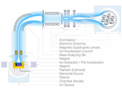
Ion Implantation
Ion implantation is a critical technique in semiconductor fabrication used to modify the electrical properties of a substrate by introducing dopants such as boron or phosphorus. This process allows for highly precise control over the concentration and placement of dopants, making it essential for forming key structures like p-n junctions in semiconductor devices.
In ion implantation, dopants are accelerated in a high-energy ion beam and implanted into the substrate at controlled depths. The energy and dosage of the ion beam determine how deep and concentrated the dopants are within the material, providing a high level of accuracy in tailoring the electrical properties of the semiconductor. This precision is especially advantageous over traditional doping methods, as it ensures uniform dopant distribution while minimizing thermal damage to the substrate.
Ion implantation is widely used in the production of transistors, diodes, and other semiconductor components where precise doping control is crucial. Its ability to achieve high levels of uniformity and depth control makes it an indispensable tool for modern semiconductor manufacturing and device performance optimization.
Semiconductor Annealing
Semiconductor annealing is an essential thermal process used in various stages of semiconductor manufacturing to modify the material properties of wafers and optimize device performance. This process involves heating a semiconductor wafer to a specific temperature and then cooling it down in a controlled manner. The key goals of annealing include repairing crystal defects, activating dopants, and relieving stresses induced by previous fabrication steps.
Types of Semiconductor Annealing
There are several types of annealing used in semiconductor manufacturing, each tailored to specific requirements:
RFHIC’s GaN solid-state microwave sources offer unique advantages for thermal processing in semiconductor annealing. By generating microwave-based plasma, these sources can enhance rapid thermal processing (RTP) and even enable new forms of annealing that are faster and more energy-efficient. Microwave-assisted annealing can be particularly useful in applications where precise thermal control is needed without inducing large thermal budgets on the wafer, thereby reducing overall processing time and increasing throughput. Techniques in next-generation devices
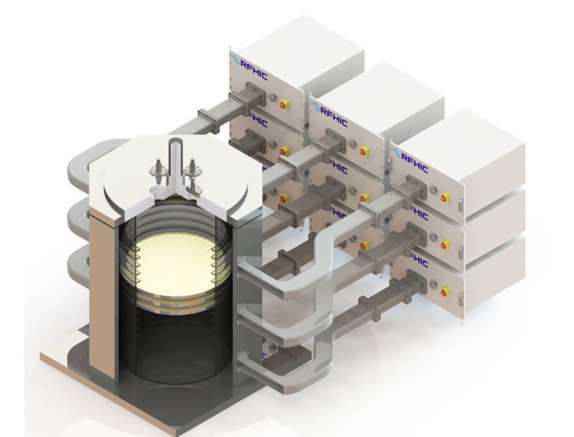
GaN Solid-State Microwave Sources in Semiconductor Manufacturing
At RFHIC, we are leveraging our deep expertise in GaN solid-state microwave sources to revolutionize semiconductor manufacturing. Our GaN solid-state microwave generators are designed to deliver higher precision, improved energy efficiency, and reduced cycle times, making them a critical tool in advanced semiconductor fabrication processes such as plasma generation, chemical vapor deposition (CVD), and rapid thermal processing (RTP).
RFHIC provides a one-stop GaN solution, offering a full suite of commercial off-the-shelf (COTS) products as well as customizable solutions to meet the diverse needs of semiconductor manufacturers.
Our COTS GaN microwave solutions include:
Click to View in Fullscreen
These solutions are designed for scalability and can be integrated into a variety of semiconductor processes, from deposition techniques like Molecular Vapor Deposition (MVD) and Atomic Layer Deposition (ALD) to thermal processing steps such as annealing and oxidation.
Customizable GaN Solutions for Specific Requirements
Beyond our COTS offerings, we also specialize in creating customizable products tailored to the unique specifications of our customers. Whether your application requires specific frequency ranges, power levels, or integration into existing systems, RFHIC can develop solutions that cater to your exact needs.
Contact Us for More Information
As the semiconductor industry continues to push the boundaries of performance and energy efficiency, RFHIC is proud to lead the way with our innovative GaN microwave solutions. If you have any questions or would like to learn more about our products and services, please fill out the form below.
Citations
Applied Materials. (2023). Deposition Technologies and Plasma-Enhanced Processes in Semiconductor Manufacturing. Available at: www.appliedmaterials.com.Semi Handbook. (2024). Semiconductor Deposition, Thermal Processing, and Ion Implantation Techniques. Semi Handbook 2nd Edition. (Document ID: file-2OXZ5OL7j1yBHisfxUcjoz4Q).Plasma Technology Document. (2024). The Role of Plasma Technology and Deposition Techniques in Semiconductor Manufacturing. (Document ID: file-krErazqhgGD0dCvuLOYK6Irp).