Wireless Infrastructure
Meeting the continually evolving demands for 4G LTE & 5G wireless infrastructure applications with RFHIC's gallium nitride (GaN) on silicon carbide (SiC) technology solutions


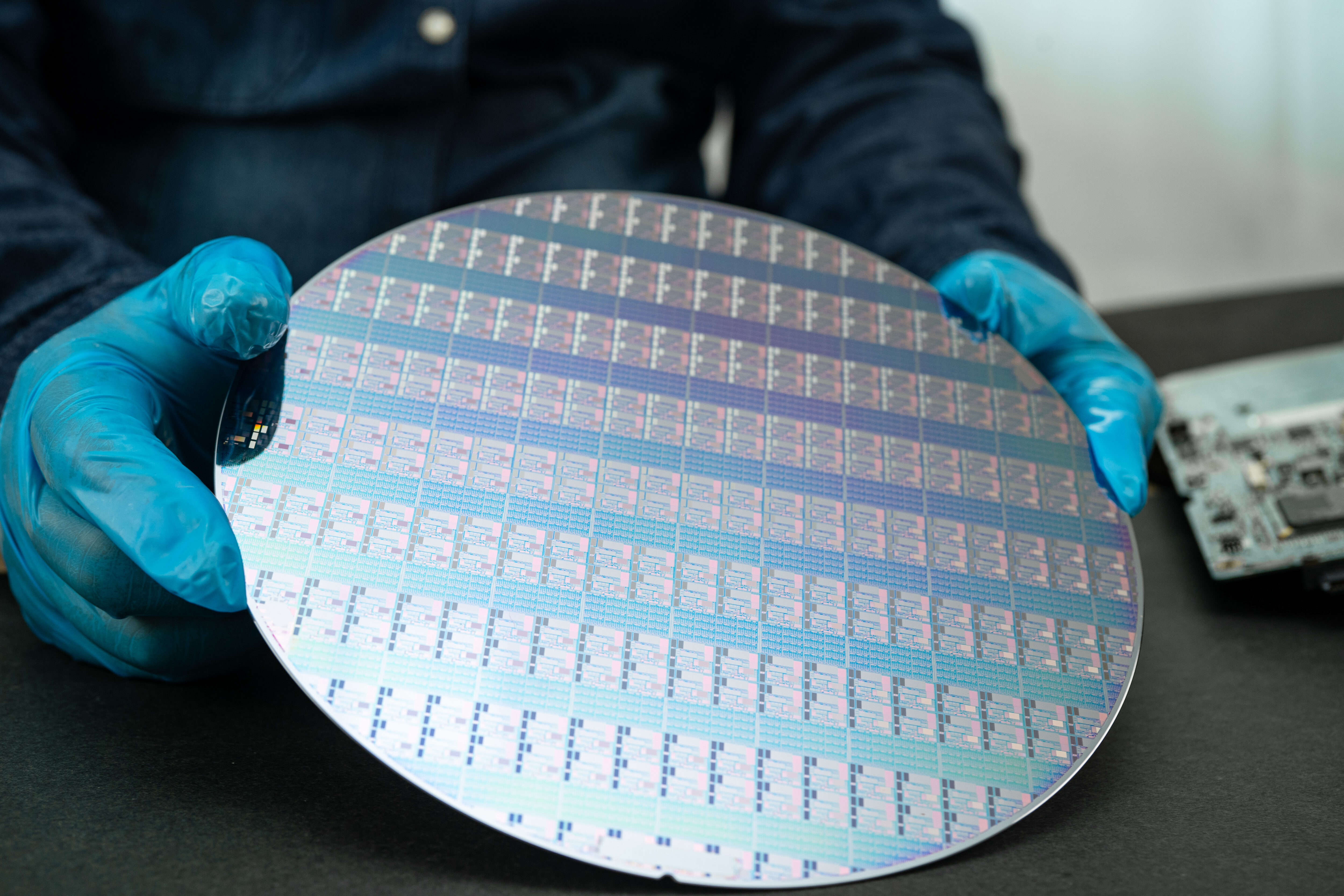
The semiconductor industry continues to expand with growing demand from AI, high-performance computing (HPC), 5G communications, and autonomous technologies. As these technologies advance, the need for higher computing performance and data processing capability continues to rise, accelerating the miniaturization and higher integration of semiconductor devices. This industry trend is placing greater emphasis on precise process control and a stable plasma environment in semiconductor manufacturing. (May & Sze, 2004; Lieberman & Lichtenberg, 2005) Plasma processes are used in a wide range of critical semiconductor manufacturing steps, including etching, thin-film deposition, and surface treatment, and they are key factors that directly influence process quality and yield. (Coburn & Winters, 1979)
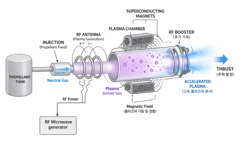
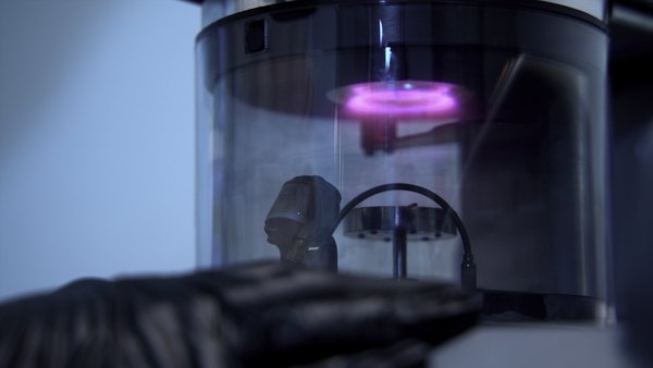
Recently, plasma generation technology using RF microwave generators has gained attention as an alternative for high-precision semiconductor processing. RF microwave equipment delivers microwave energy into process gases to create a plasma state in which electrons and ions are generated, thereby enabling a variety of chemical reactions. In particular, microwave-based plasma offers high energy coupling efficiency and uniform plasma formation. (Lieberman & Lichtenberg, 2005) In addition, this approach can be implemented with low or no electrode dependence, which is advantageous in reducing process contamination and improving equipment lifetime.
High-density plasma can be used to form fine patterns with precision and is particularly effective for etching high-aspect-ratio structures. This plasma etching technology has become one of the core technologies enabling semiconductor miniaturization. (Coburn & Winters, 1979)
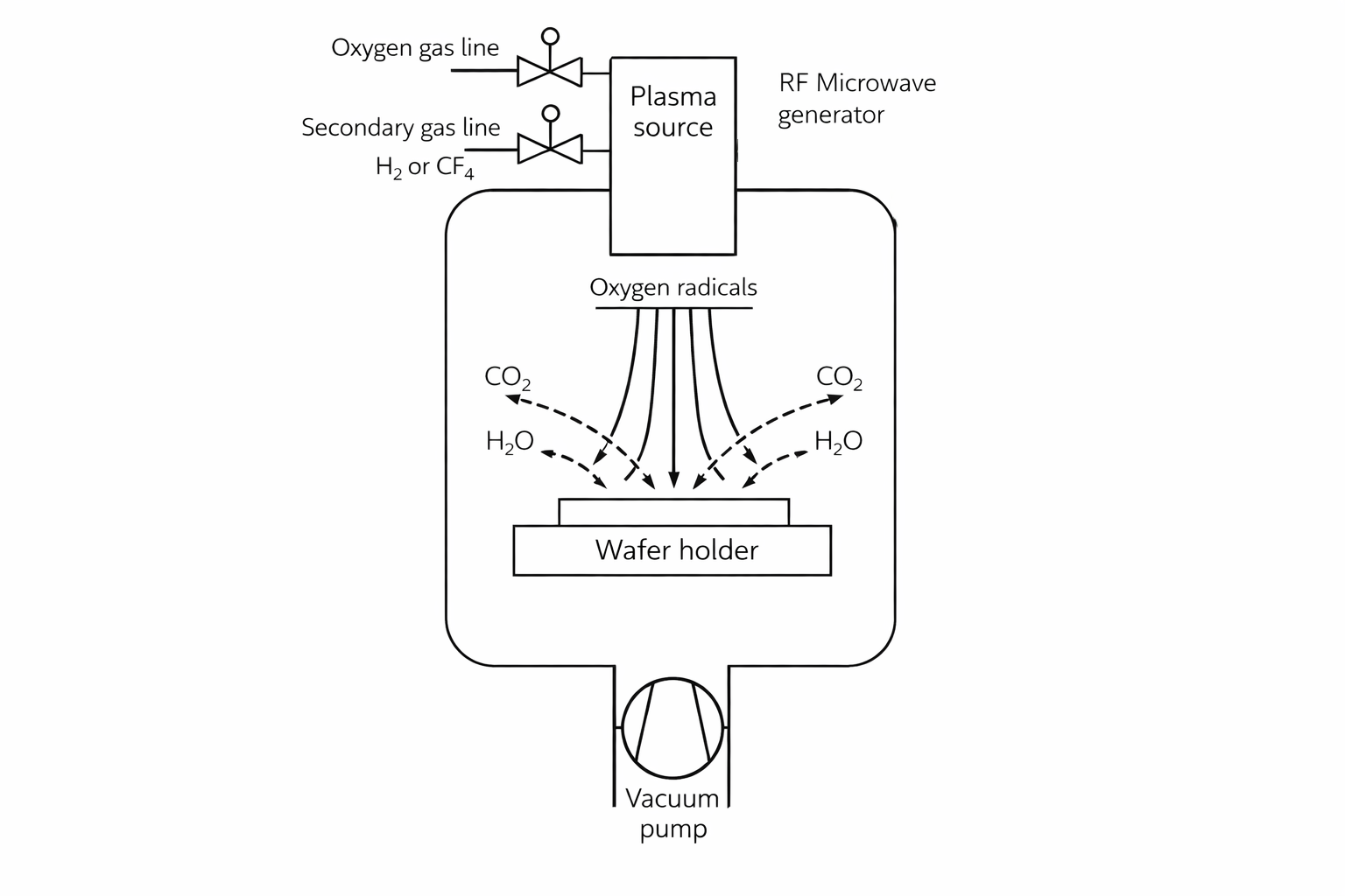
Plasma-enhanced chemical vapor deposition (PECVD) uses plasma to enable stable thin-film formation even at lower temperatures. RF microwave-based plasma can contribute to uniform film thickness and the formation of high-quality thin films. (Ohring, 2002)
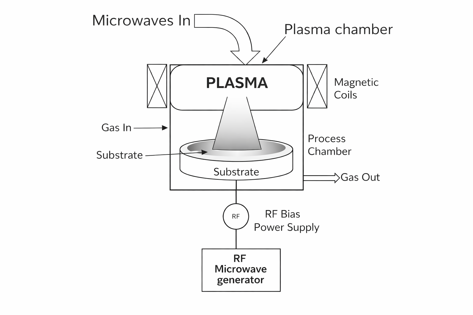
Plasma-based surface activation is used to improve material adhesion, control surface energy, and enhance electrical properties. In particular, microwave-based plasma enables uniform surface modification, making it suitable for high-precision processes.
The performance of plasma processes depends heavily on the stability and precise controllability of the RF power source used to generate the plasma. A stable RF microwave generator plays a critical role in maintaining consistent plasma density, ion energy, and reaction uniformity, making it a key factor in ensuring process repeatability and equipment reliability. (Lieberman & Lichtenberg, 2005) In advanced semiconductor processes, where nanometer-level control is required, fine RF power tuning is considered essential.
| Output Power | Application | Notes |
|---|---|---|
| 100 W | Research and Small-Scale Processes | Lab / R&D |
| 200 W | Pilot Processes | Pilot |
| 500 W | Volume Manufacturing | Production |
| 800 W+ | High-Density Processes | Advanced |
| Part Number | Min Freq (MHz) |
Max Freq (MHz) |
Output Power (W) |
VDC (V) |
Cooling | Dimension (mm) |
Operating Mode |
DC RF Efficiency (%) |
VSWR | Interface | Line Connection |
|---|---|---|---|---|---|---|---|---|---|---|---|
| RIM25100-20G | 2400 | 2500 | 100 | 50 | Air | 200×100×30 | CW/Pulse | 60 | 6:01 | RS-232 | D-Sub 7W2 |
| RIM25200-20G | 2400 | 2500 | 200 | 50 | Air | - | CW/Pulse | 60 | 6:01 | RS-232 | D-Sub 7W2 |
| RIM25500-20G | 2400 | 2500 | 500 | 50 | Water | - | CW/Pulse | - | - | RS-232 | D-Sub 7W2 |
| RCM25800-20G | 2400 | 2500 | 800 | 50 | Water | 320×150×51 | CW/Pulse | - | - | - | - |
| RCM251K6-20G | 2400 | 2500 | 1600 | 50 | Water | 200×362×53 | CW/Pulse | 57 | 6:01 | RS-232 | D-sub 5W5 |
Plasma technology based on RF microwave generators is expected to play an important role in next-generation semiconductor processing due to its advantages, including high plasma density, excellent process stability, and low contamination characteristics. In particular, as a technology capable of meeting the precise control requirements of fine-process and highly integrated semiconductor manufacturing, it is likely to become a core enabling technology in future semiconductor manufacturing equipment.
References
Lieberman, M. A., & Lichtenberg, A. J. (2005).
Principles of Plasma Discharges and Materials Processing (2nd ed.).
Wiley-Interscience.
Chen, F. F. (2016).
Introduction to Plasma Physics and Controlled Fusion.
Springer.
Coburn, J. W., & Winters, H. F. (1979).
Ion- and electron-assisted gas-surface chemistry—An important effect in plasma etching.
Journal of Applied Physics, 50(5), 3189–3196.
Ohring, M. (2002).
Materials Science of Thin Films (2nd ed.).
Academic Press.
May, G. S., & Sze, S. M. (2004).
Fundamentals of Semiconductor Fabrication.
Wiley.