Wireless Infrastructure
Meeting the continually evolving demands for 4G LTE & 5G wireless infrastructure applications with RFHIC's gallium nitride (GaN) on silicon carbide (SiC) technology solutions


By 2026, the success of your massive MIMO deployment depends less on raw signal strength and more on how effectively you manage heat at the transistor level. While GaN-on-Silicon was once a viable entry point, the thermal demands of modern 5G wireless infrastructure GaN applications have rendered it obsolete for high-performance base stations. You've likely already faced the frustrations of thermal throttling in high-density arrays or the prohibitive weight of massive heat sinks required to keep sub-6GHz systems stable. These aren't just engineering inconveniences; they're fundamental barriers to scaling network capacity.
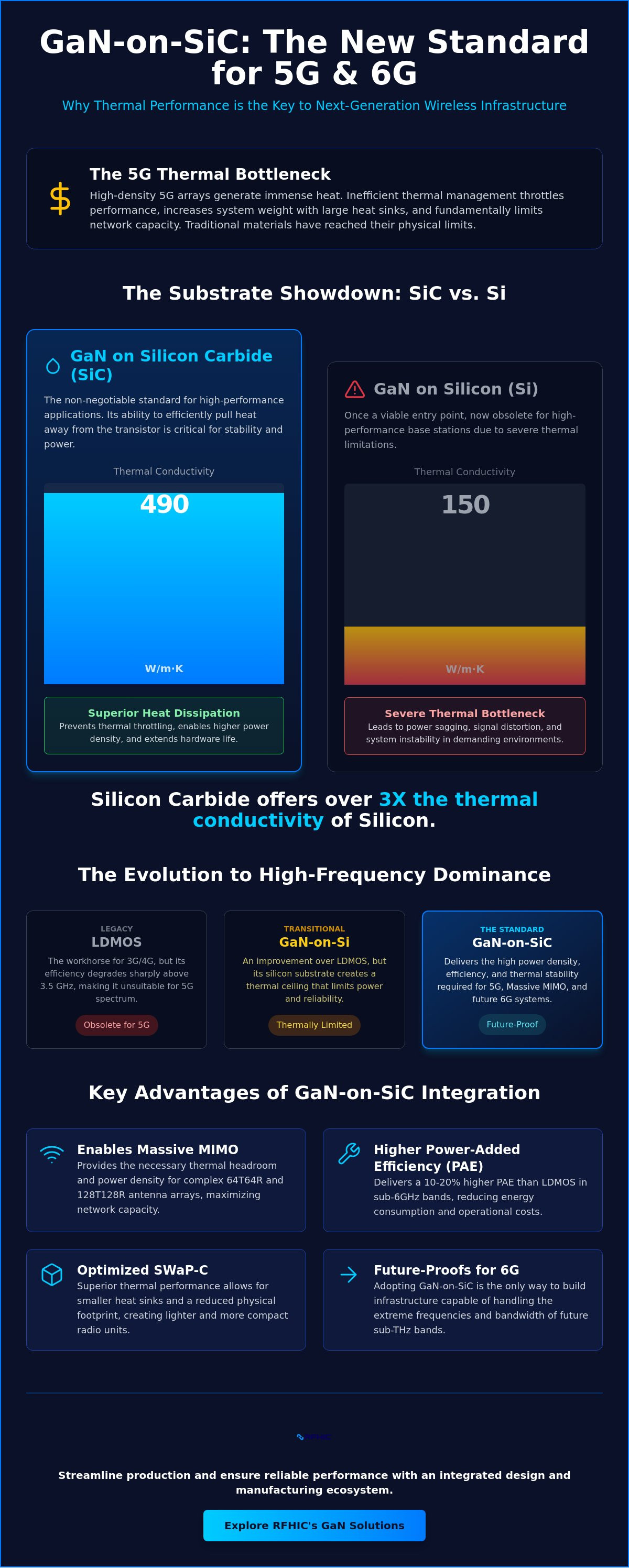
This article demonstrates why GaN-on-SiC has become the non-negotiable standard for engineers who need to maximize power-added efficiency and reduce unit weight. We'll analyze the critical performance gap between Silicon Carbide and Silicon substrates, focusing on SiC's superior thermal conductivity of up to 490 W/m·K compared to the mere 150 W/m·K offered by Si. You'll discover how choosing the right substrate allows for a significant reduction in footprint while future-proofing your systems for the upcoming transition to 6G frequencies. We'll provide a technical roadmap for optimizing SWaP-C through advanced GaN-on-SiC integration.
For decades, Laterally Diffused Metal Oxide Semiconductor (LDMOS) technology served as the undisputed workhorse of cellular base stations. It provided reliable, cost-effective performance for 3G and 4G LTE networks operating primarily at frequencies below 2.5 GHz. However, the architectural requirements of 5G have fundamentally altered the design landscape. Modern 5G wireless infrastructure GaN solutions have emerged as the only viable path forward as network operators push into higher spectrum bands to accommodate massive data throughput. Traditional silicon has reached its physical limits.
The global surge in 5G data traffic exerts immense pressure on Radio Access Network (RAN) power amplifiers. To maintain signal integrity across wider bandwidths, engineers have turned to High Electron Mobility Transistors (HEMT). These devices leverage the unique properties of Gallium nitride (GaN) to deliver high-speed switching and superior power density. Unlike LDMOS, which struggles with parasitic capacitance at higher frequencies, GaN HEMTs maintain high gain and efficiency even as the spectrum expands into the sub-6 GHz and millimeter-wave (mmWave) regions. This transition isn't just an upgrade; it's a necessity for survival in a high-capacity environment.
GaN is a wide bandgap (WBG) semiconductor, meaning it requires significantly more energy to move electrons from the valence band to the conduction band than silicon. This property results in a much higher breakdown voltage, allowing devices to operate at higher voltages without failure. Higher voltage operation directly correlates to increased power density, enabling smaller components to do the work of much larger silicon counterparts. The wide bandgap of GaN enables 5G systems to operate at significantly higher voltages and temperatures than silicon, effectively tripling the power density available for power amplification.
In the critical sub-6GHz bands, Power-Added Efficiency (PAE) is the metric that determines operational viability. LDMOS efficiency begins to degrade sharply as frequencies move past 3.5 GHz, leading to excessive heat generation. This creates a bottleneck for massive MIMO (mMIMO) arrays, which utilize 64T64R or 128T128R configurations. Packing dozens of inefficient silicon amplifiers into a single radio unit results in thermal loads that traditional cooling systems can't manage. 5G wireless infrastructure GaN technology solves this by providing 10% to 20% higher PAE than LDMOS at these frequencies. This efficiency gain allows for smaller heat sinks and lighter overall units, which is essential for rooftop and pole-mounted installations where weight and size are strictly regulated.
While some manufacturers promote GaN-on-Silicon (GaN-on-Si) as a scalable, high-volume alternative, this approach often overlooks the critical thermal constraints of high-density networks. The strategic selection of substrates for 5G wireless infrastructure GaN systems determines the upper limit of network performance. Silicon Carbide (SiC) provides a superior foundation that manages the extreme heat generated by high-frequency power amplifiers. Choosing Si over SiC might reduce initial wafer costs, but it introduces significant thermal bottlenecks that compromise the entire system's efficiency.
The core of the debate lies in thermal conductivity. Silicon Carbide exhibits a thermal conductivity of approximately 400 W/mK, whereas Silicon is limited to roughly 150 W/mK. This nearly 3x difference means that SiC-based devices can dissipate heat far more effectively than their Si-based counterparts. The widespread adoption of GaN semiconductors in 5G has validated this performance gap. When heat builds up at the transistor junction, it leads to power sagging and signal distortion. SiC’s ability to pull heat away from the active region keeps the device running cooler, which preserves signal linearity and extends the hardware's operational life.
Thermal management isn't just about cooling; it's about reliability. High-heat environments accelerate degradation, directly impacting the Mean Time to Failure (MTTF) of base station components. By utilizing GaN-on-SiC, operators can reduce the size and complexity of cooling hardware, such as bulky heat sinks and active fans. This reduction is vital for urban deployments where space is at a premium. Engineers seeking to minimize thermal resistance often turn to specialized GaN on SiC transistors to maintain peak performance under heavy traffic loads.
Power density is measured in Watts per millimeter (W/mm) of gate periphery. GaN-on-SiC consistently delivers higher power density than GaN-on-Si, allowing for smaller transistor footprints without sacrificing output. This high-power density is critical for shrinking 5G base station dimensions and enabling the integration of more antenna elements in massive MIMO arrays. Optimizing 5G wireless infrastructure GaN designs requires a shift from component-level cost analysis to a Total Cost of Ownership (TCO) perspective. While Si wafers are cheaper, the system-level savings in electricity, cooling, and maintenance make SiC the more economical choice over the long term.
In 2026, the success of high-density network deployments hinges on optimizing SWaP-C: Size, Weight, Power, and Cost. As the massive MIMO market is projected to reach USD 8.4 billion this year, the pressure on hardware manufacturers to deliver more capacity in smaller packages has intensified. Transitioning to 64T64R and 128T128R antenna arrays requires an unprecedented concentration of power amplifiers within the Radio Unit (RU). Traditional silicon-based solutions cannot meet these requirements. They are simply too heavy and inefficient to stay within the strict weight limits of existing telecom towers. By contrast, 5G wireless infrastructure GaN technology provides the power density required to pack high-element arrays into compact, lightweight enclosures.
Integrating advanced materials for 5G like GaN-on-SiC directly addresses the physical bottlenecks of massive MIMO. It allows for a radical reduction in heat sink volume, which leads to a cascading series of benefits. Lighter units reduce the structural reinforcement costs for towers. Higher efficiency reduces the monthly utility bills for carriers. When every watt saved translates into lower OpEx, the economic argument for GaN-on-SiC becomes undeniable. This material efficiency is the primary reason why 5G is expected to be the fastest-growing segment with a CAGR of 23.94% through 2035.
Miniaturization is the core objective for modern deployments. By integrating GaN MMICs into front-end modules, manufacturers achieve a significant reduction in footprint. Recent industry developments have focused on integrated GaN package designs that specifically target the needs of 5G Radio Units. These designs improve cost efficiency while simultaneously reducing the physical load on tower infrastructure. High-efficiency 5G wireless infrastructure GaN components ensure that carriers don't have to choose between network capacity and operational sustainability. This streamlined approach to hardware design is essential for the rapid rollout of urban small cells.
Maintaining signal purity across wide bandwidths is a complex engineering challenge. High-power GaN devices must exhibit excellent linearity to work effectively with Digital Pre-Distortion (DPD) algorithms. Without this linearity, signal distortion would bleed into adjacent channels and violate regulatory standards. RFHIC’s specialized GaN on SiC Transistors for wireless infrastructure provide a distinct advantage here. They offer the electron mobility and breakdown voltage necessary to handle wideband signals without compromising integrity. This ensures that even as bandwidth requirements grow toward the 6G era, the infrastructure remains stable, reliable, and compliant.
The roadmap toward 6G begins long before the first commercial networks go live in 2030. While 2026 represents the peak of 5G Advanced deployments, the engineering focus is already shifting toward the D-band (110-170 GHz) and sub-THz frequencies. These extreme spectral regions demand semiconductors with significantly higher electron mobility and power density than current standards. While existing 5G wireless infrastructure GaN solutions successfully navigate the sub-6 GHz and early mmWave bands, 6G introduces unprecedented path loss challenges. Overcoming these requires a material foundation that doesn't just manage heat, but thrives under extreme power levels.
GaN-on-SiC remains the primary engine for this transition. It provides the necessary bandwidth and efficiency to sustain signal integrity at frequencies where silicon-based alternatives fail. For the most demanding ultra-high-power 6G applications, the industry is exploring GaN-on-Diamond. Diamond’s thermal conductivity is several times higher than even Silicon Carbide. This offers a potential path to manage the intense heat generated by sub-THz range extension. This evolution ensures that the infrastructure remains scalable and reliable as data demands continue to climb. By 2030, GaN will be the primary semiconductor enabling commercial 6G sub-THz links and intelligent, AI-managed radio access networks.
Moving beyond the 24 GHz ceiling requires extreme power at mmWave and sub-THz levels to compensate for atmospheric absorption. Path loss is the primary enemy of 6G. Engineers must deploy high-gain, high-power amplifiers to maintain link budgets over meaningful distances. RFHIC is currently evolving its technology to meet these sub-THz requirements, focusing on maximizing gain at the device level. This specialized hardware is essential for bridging the gap between current 5G capacity and the terabit-per-second goals of 6G. To prepare for these next-generation spectral demands, explore our high-performance GaN on SiC transistors for infrastructure applications.
6G base stations will utilize artificial intelligence to manage energy consumption dynamically. This requires power amplifiers that can switch states rapidly without losing efficiency. The synergy between GaN’s high switching speed and AI-managed beamforming allows networks to scale power output in real-time based on user traffic. This reduces wasted energy during low-traffic periods while maintaining peak performance during surges. 5G wireless infrastructure GaN technology provides the agility needed for these intelligent, self-optimizing networks. As AI becomes deeply integrated into the Radio Access Network (RAN), the rapid response times of GaN-on-SiC will be a critical enabler of network-wide power savings.
While previous sections established the thermal and efficiency advantages of the material, the practical implementation of 5G wireless infrastructure GaN requires a partner with end-to-end manufacturing control. RFHIC operates as a singular source of truth in the semiconductor landscape. We maintain total oversight from the initial transistor design to the final assembly of complete transmitter systems. This vertical integration eliminates the fragmentation often found in global supply chains. It ensures that every component meets the rigorous standards required for 2026 deployments. Our internal design and manufacturing capabilities allow for rapid prototyping and precise quality control. We don't just provide parts. We deliver integrated solutions that solve the specific bottlenecks of modern Radio Access Networks. This mastery of the craft positions RFHIC as a dependable partner for OEMs who cannot afford the risks of multi-vendor dependencies.
The ecosystem begins with our high-performance GaN on SiC Transistors for Wireless Infrastructure. These discrete components provide the foundation for high-gain, high-efficiency amplification. However, we also provide GaN Solid-State Power Amplifiers (SSPAs) as complete, ready-to-integrate base station modules. This flexibility allows telecom OEMs to choose the level of integration that fits their specific architecture. By controlling the entire process, we ensure that the thermal management strategies discussed earlier are baked into the hardware at every level. Our internal control allows us to optimize the interface between the transistor and the heat sink, maximizing the 490 W/m·K thermal conductivity potential of the SiC substrate.
Every carrier operates on unique frequency bands and under specific environmental constraints. We offer comprehensive OEM Services to address these variations. Our engineering teams collaborate directly with clients to develop custom GaN solutions tailored to specialized 5G and future 6G requirements. This collaborative approach leverages our extensive experience in defense-telecom dual-use technology. The same reliability required for high-stakes radar systems is applied to commercial wireless infrastructure. This cross-industry expertise ensures that our hardware performs under the most demanding conditions. For manufacturers looking to secure their roadmap through 2030, the choice of a technology partner is critical. We provide the stability, innovation, and high-volume production capacity necessary to lead the market. Explore RFHIC’s GaN on SiC solutions for 5G and 6G to see how our integrated ecosystem can streamline your next deployment.
The transition from silicon-based legacy systems to high-performance GaN-on-SiC is no longer a matter of preference; it's a structural requirement for 2026 and beyond. As established throughout this analysis, the superior thermal conductivity of Silicon Carbide is the only viable method for managing the extreme power densities of massive MIMO and sub-THz frequencies. By prioritizing SWaP-C optimization today, you're building a foundation that can scale into the 6G era without the need for frequent hardware overhauls. High-efficiency 5G wireless infrastructure GaN solutions provide the reliability and performance density required to meet the world's exponential data demands.
RFHIC brings over 20 years of GaN innovation to every partnership, serving as a trusted global supplier to Tier-1 telecom and defense OEMs. Our proprietary GaN on SiC technology ensures that your systems remain stable under the most demanding thermal loads while reducing overall unit weight. We invite you to leverage our end-to-end design and manufacturing ecosystem to streamline your deployment and maximize network capacity. Partner with RFHIC for your next-generation 5G GaN infrastructure and take control of your technical roadmap. The path to a faster, more efficient network starts with a commitment to superior semiconductor materials.
GaN-on-SiC is preferred because it offers significantly higher thermal conductivity, typically ranging from 330 to 490 W/m·K. This is nearly triple the performance of GaN-on-Silicon, which is limited to approximately 150 W/m·K. In high-power 5G environments, this superior heat dissipation allows for higher power density and prevents the thermal throttling that often degrades signal quality in silicon-based substrates.
GaN technology improves efficiency by delivering a higher Power-Added Efficiency (PAE) than traditional LDMOS. By converting a larger percentage of DC power into RF energy, GaN reduces the amount of power wasted as heat. This efficiency is vital for 5G wireless infrastructure GaN applications, as it directly lowers the electricity consumption of base stations and reduces the cooling requirements for dense network deployments.
In Massive MIMO arrays, GaN acts as the primary enabler for high-element configurations such as 64T64R and 128T128R. Its high power density allows engineers to pack dozens of power amplifiers into a compact radio unit. This miniaturization is essential for maintaining a manageable footprint while delivering the massive data throughput and beamforming capabilities required for urban 5G coverage.
Yes, GaN-on-SiC is uniquely suited for the sub-THz and D-band frequencies expected in the 6G era. The material's high electron mobility and breakdown voltage allow it to maintain gain and efficiency at frequencies well above 100 GHz. This makes it a critical foundation for overcoming the extreme path loss challenges associated with the next generation of wireless communication.
GaN-on-SiC facilitates a significant reduction in both size and weight by minimizing the volume of cooling hardware. Because the material operates efficiently at higher temperatures and dissipates heat effectively, manufacturers can use smaller heat sinks. This weight reduction is critical for tower-mounted equipment, where structural load limits often restrict the installation of heavier, silicon-based radio units.
The primary advantage of a Silicon Carbide (SiC) substrate is its ability to pull heat away from the transistor junction with extreme efficiency. This prevents the formation of localized hot spots that can lead to device failure or performance degradation. By maintaining lower operating temperatures, SiC substrates ensure that the transistors achieve a longer Mean Time to Failure (MTTF) in demanding environments.
GaN-on-SiC is fully compatible with advanced Digital Pre-Distortion (DPD) techniques used to maintain signal linearity. Its predictable performance across wide bandwidths allows DPD algorithms to effectively correct for nonlinearities. This synergy is essential for 5G wireless infrastructure GaN systems to meet strict regulatory standards for signal purity and adjacent channel leakage ratios.
RFHIC supports telecom OEMs through an integrated ecosystem that includes discrete transistors, power amplifier modules, and complete transmitter systems. We offer specialized OEM Services to provide custom hardware tailored to specific frequency bands and power requirements. Our end-to-end control over the design and manufacturing process ensures supply chain reliability and technical excellence for high-volume infrastructure projects.