Wireless Infrastructure
Meeting the continually evolving demands for 4G LTE & 5G wireless infrastructure applications with RFHIC's gallium nitride (GaN) on silicon carbide (SiC) technology solutions






RFHIC today launched DiaFlux™, a family of thermal-grade polycrystalline CVD diamond heat spreaders for high-power RF, microwave, optoelectronic, and semiconductor packaging applications. The DiaFlux™ product pages, including full specifications for both grades, are now live on RFHIC’s website. [https://rfhic.com/products-diamond-materials/]
Modern high-power designs concentrate ever-greater heat flux beneath small, high-power die. When conventional heat-spreader materials become the bottleneck, the design’s thermal ceiling caps output power, density, and performance. DiaFlux™ brings the highest-thermal-conductivity material class in engineering practice directly to the point of heat generation — in the sizes, thicknesses, and tolerances real packages need.
The family launches with two grades sharing one form-factor system:
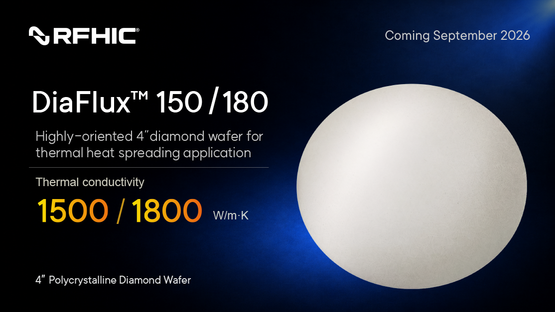
Key specifications (both grades):
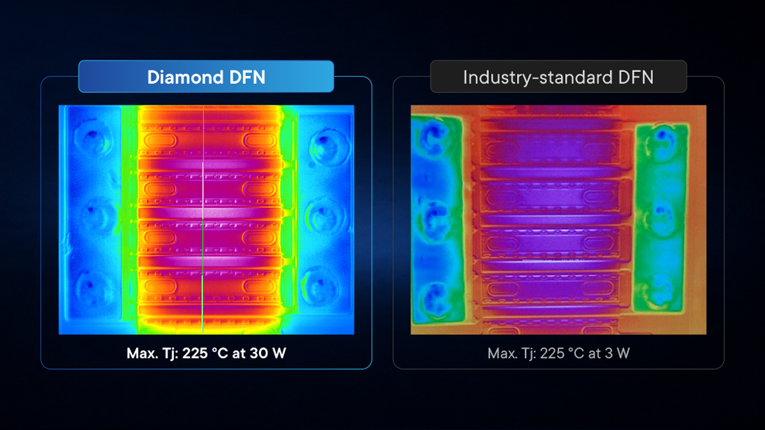
Because both grades share identical form factors, thickness, tolerances, and surface finish, grade selection is purely a thermal-performance decision — switching grades does not change the mechanical design.
Getting started
Engineers evaluating a thermal design can request a technical consultation with RFHIC’s application engineering team through the DiaFlux™ product pages. To learn more, please contact us.
About RFHIC
RFHIC (KOSDAQ: A218410) is a global leader in GaN RF and microwave solutions, specializing in wireless communications, defense, aerospace, and industrial RF energy applications. The company develops and manufactures high-power GaN transistors, MMICs, solid-state power amplifiers, and microwave generator systems, all produced in-house for superior quality and performance. RFHIC is committed to advancing next-generation power semiconductor technologies to create a more connected, energy-efficient, and innovative future. Learn more at www.rfhic.com.
RFHIC® is a registered trademark.
For more information, please contact:
RFHIC Corporation — Global Sales & Marketing — Email: marketing@rfhic.com
[News] RFHIC Announces DiaFlux™ Thermal-Grade CVD Diamond Heat Spreaders, Coming September 2026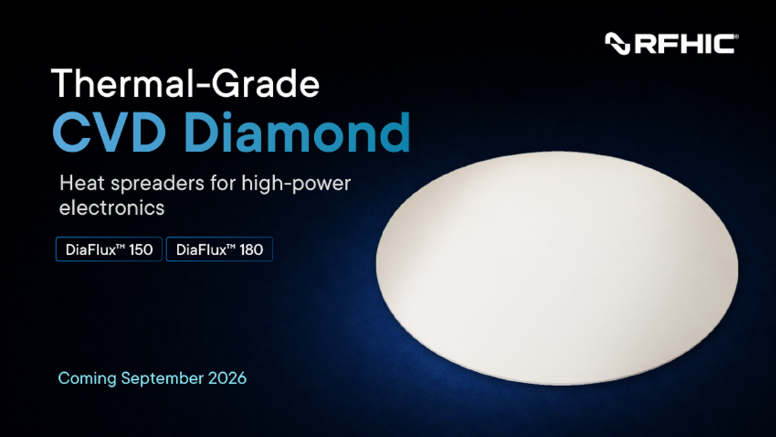
RFHIC will launch DiaFlux™, a family of thermal-grade polycrystalline CVD diamond heat spreaders developed for high-power RF, microwave, optoelectronic, and semiconductor packaging applications. Full product specifications and product pages will go live on Tuesday, September 8, 2026.
For two decades, RFHIC has designed and manufactured GaN RF and microwave devices — components whose performance depends on how quickly heat leaves a millimeter-scale die. As power densities continue to rise across telecom, radar, RF energy, laser, and advanced packaging applications, the thermal performance of the first layer beneath the device increasingly determines the thermal budget of the entire system. DiaFlux™ applies RFHIC’s device-level thermal understanding to the material itself.
The DiaFlux™ family will launch with two grades:
Both grades are grown by plasma-assisted chemical vapor deposition, are electrically insulated, and will be offered in engineered geometries spanning chips, plates, heat spreaders, and wafers — including custom formats. Complete dimensional specifications, tolerances, and surface-finish data will be published at launch.
If interested in learning more about RFHIC’s DiaFlux™ technology, please contact us at www.rfhic.com/contact
About RFHIC
RFHIC (KOSDAQ: A218410) is a global leader in GaN RF and microwave solutions, specializing in wireless communications, defense, aerospace, and industrial RF energy applications. The company develops and manufactures high-power GaN transistors, MMICs, solid-state power amplifiers, and microwave generator systems, all produced in-house for superior quality and performance. RFHIC is committed to advancing next-generation power semiconductor technologies to create a more connected, energy-efficient, and innovative future. Learn more at www.rfhic.com.
RFHIC® is a registered trademark.
Pulsed RF Power Amplifier: The GaN-on-SiC Guide to Modern Radar PerformanceCan a solid-state architecture truly match the raw peak power of a traveling wave tube while eliminating the thermal throttling that often limits a pulsed RF power amplifier in high-duty-cycle radar? For decades, engineering teams in the defense and aerospace sectors accepted the excessive weight and frequent maintenance cycles of legacy vacuum tubes as an unavoidable trade-off. It’s a persistent challenge to maintain system reliability when your hardware is prone to failure and requires complex, bulky cooling systems to stay operational.
This guide explores how GaN-on-SiC technology is fundamentally redefining modern transmitter design by delivering unmatched thermal conductivity and pulse fidelity. With GaN-on-SiC technology projected to hold a 70% share of the GaN RF market in 2026, the industry is rapidly pivoting toward these more resilient, solid-state architectures. You’ll learn how to leverage GaN-on-SiC to achieve superior SWaP-C efficiency and improve Mean Time Between Failures (MTBF) in high-stakes environments. We provide a technical breakdown of precise pulse shaping for digital radar, showing you how to move beyond the limitations of legacy systems to secure a decisive performance advantage.
A pulsed RF power amplifier is a specialized electronic component engineered to amplify radio frequency signals in short, intense bursts rather than a continuous stream. Unlike continuous wave (CW) amplifiers that provide a steady output, pulsed systems concentrate energy into microsecond or millisecond intervals. This operational mode is foundational for modern detection systems. By delivering massive peak power during the “on” state and remaining silent during the “off” state, these amplifiers allow sensitive receivers to capture faint return signals without interference from the transmitter itself.
In 2026, the technology has reached a critical inflection point. The global industry is rapidly moving away from legacy magnetrons and Traveling Wave Tubes (TWTs) in favor of Solid-State Power Amplifiers (SSPAs). This shift is driven by the requirement for higher resolution and longer range in contested electromagnetic environments. An RF power amplifier optimized for pulsed operation is now essential across multiple high-stakes sectors. Defense agencies utilize them for Electronic Warfare (EW) and jamming; aerospace firms integrate them into satellite communications; and scientific institutions rely on them to drive particle accelerators with extreme precision.
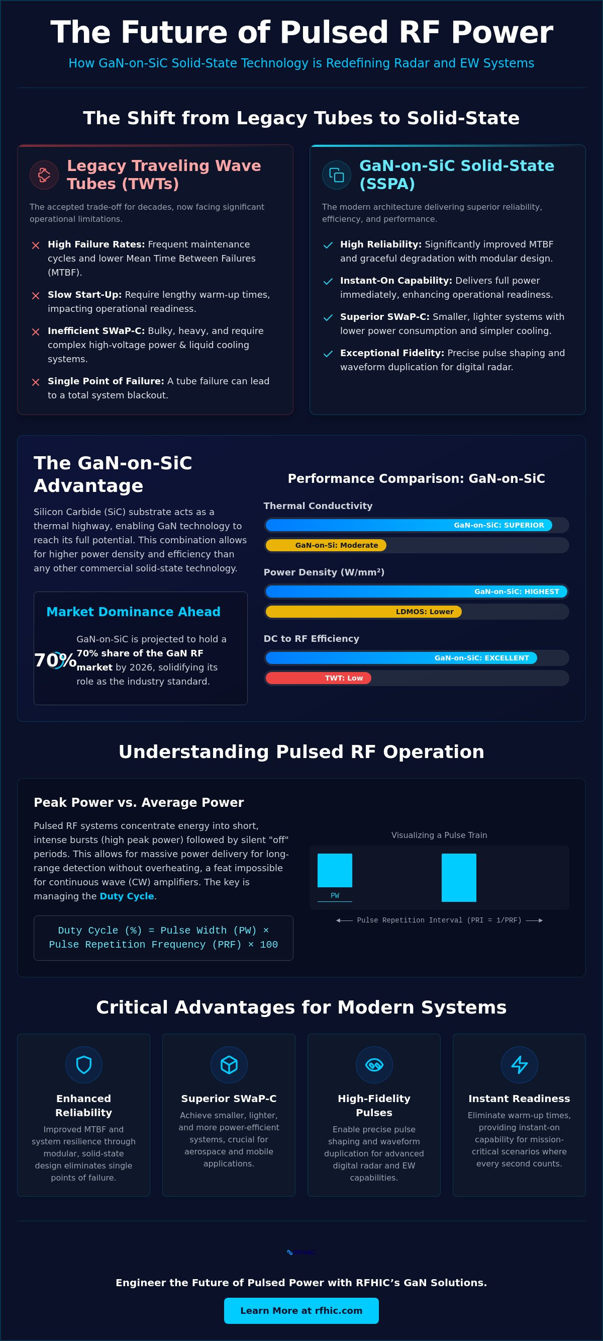
The performance of a pulsed system isn’t measured by its average output alone. Instead, engineers focus on peak power density. The relationship between the “on” time and the total cycle is defined as the Duty Cycle. It’s calculated using the Pulse Width (PW) and the Pulse Repetition Frequency (PRF). A low duty cycle allows the system to reach much higher peak power levels than would be possible in CW mode without damaging the internal circuitry. In modern radar, mastering this balance is the primary KPI for achieving maximum target detection range while maintaining thermal stability. It’s no longer just about raw energy; it’s about how effectively that energy is partitioned.
The evolution from Silicon LDMOS to Gallium Nitride (GaN) has fundamentally changed the preferred architecture for S-band and X-band radar. Solid-state technology offers a significant reliability advantage by eliminating the need for high-voltage power supplies and fragile vacuum seals found in legacy tubes. Because GaN-on-SiC devices provide superior power density and thermal conductivity, they’ve become the standard for high-performance systems. These amplifiers don’t require lengthy warm-up times. They deliver instant-on capability and modularity, ensuring that a single component failure doesn’t result in a total system blackout. This transition to solid-state is a total reimagining of system uptime and operational readiness.
Material properties dictate the performance boundaries of any high-frequency system. While Gallium Nitride (GaN) provides the high breakdown voltage and electron mobility required for amplification, the substrate beneath it determines how well the device survives extreme stress. Silicon Carbide (SiC) has emerged as the superior substrate for a pulsed RF power amplifier because it acts as a thermal highway. Unlike GaN-on-Silicon or legacy LDMOS, GaN-on-SiC allows for significantly higher power density, often achieving more Watts per square millimeter than any other commercially available solid-state technology. This density isn’t just a vanity metric; it enables engineers to shrink the overall system footprint while reducing the complexity of liquid or forced-air cooling infrastructures.
The efficiency gains realized through this architecture are substantial. By converting a higher percentage of DC power into RF energy, GaN-on-SiC minimize wasted heat. This is particularly vital when generating complex Pulsed RF waveforms that require rapid switching and high peak output. For teams designing modern radar suites, these advancements mean smaller, lighter, and more mobile units that don’t sacrifice range or sensitivity. To see how these material benefits translate into hardware, explore our range of GaN-on-SiC transistors designed for high-power defense applications.
In high-duty-cycle radar, the primary enemy is the junction temperature spike. During a long pulse, heat builds up rapidly within the High Electron Mobility Transistor (HEMT) structure. If this heat isn’t evacuated instantly, thermal resistance leads to performance degradation or catastrophic failure. Silicon Carbide offers a thermal conductivity nearly three times higher than traditional Silicon, enabling rapid heat dissipation away from the active device region. This superior thermal management ensures long-term HEMT reliability even when the system is pushed to its absolute operational limits.
Modern electronic warfare requires amplifiers that maintain strict linearity across broad frequency ranges. GaN-on-SiC excels here by minimizing pulse droop, a phenomenon where the power level sags during the duration of a single pulse. For high-resolution Synthetic Aperture Radar (SAR), maintaining phase noise stability and signal purity is non-negotiable. Custom GaN designs allow for precise control over these variables, ensuring that the amplified waveform is a near-perfect duplicate of the input signal. This fidelity is what allows digital radar systems to distinguish between closely spaced targets in cluttered environments.
Choosing between a Solid-State Power Amplifier (SSPA) and a Traveling Wave Tube (TWT) is no longer a simple question of raw wattage. For decades, TWTs were the only viable option for a pulsed RF power amplifier requiring high peak power at microwave frequencies. However, the maturation of GaN-on-SiC technology has shifted the decision framework toward solid-state architectures. This transition isn’t just about replacing a component; it’s about moving from a vacuum-based, high-maintenance system to a modular, semiconductor-driven platform that offers vastly superior longevity.
Reliability metrics highlight the most stark contrast. TWTs rely on thermionic emission, which involves heating a cathode to extreme temperatures within a vacuum. This process is inherently life-limited. In contrast, GaN-on-SiC SSPAs utilize semiconductor physics, offering a Mean Time Between Failures (MTBF) that often exceeds TWTs by an order of magnitude. While a vacuum tube might fail catastrophically due to a seal breach or cathode exhaustion, a solid-state system continues to perform reliably for years without the need for scheduled replacements.
Operational readiness is another critical differentiator in defense environments. TWT systems require significant warm-up times, often several minutes, to reach thermal equilibrium before they can transmit. In a mission-critical radar application, this delay is unacceptable. Solid-state amplifiers provide instant-on capability for any pulsed RF power amplifier configuration. They’re ready to transmit the moment they receive power. When you factor in the energy efficiency of GaN, the Total Cost of Ownership (TCO) begins to favor SSPAs. Reduced energy consumption and the elimination of frequent downtime for tube swaps make solid-state the more economical choice over the system’s full lifecycle.
The most significant engineering advantage of solid-state systems is their modularity. TWTs are binary; if the tube fails, the entire transmitter goes dark. SSPA architectures utilize multiple combined modules. If a single GaN-on-SiC MMIC or power module fails, the system experiences “graceful degradation.” The output power drops slightly, but the radar remains operational. This soft failure mode provides a critical safety net in mission-critical defense environments where total system failure isn’t an option.
Size, weight, and power (SWaP) are the primary constraints for mobile radar units. GaN-on-SiC technology enables a reduction in footprint by eliminating the bulky, high-voltage power supplies required by TWTs. Because these devices operate at higher efficiencies, they generate less waste heat per watt of RF output. This allows for the transition from complex, heavy liquid-cooled systems to streamlined, air-cooled designs. In 2026, this optimization is essential for deploying high-power radar on smaller, agile platforms without compromising on performance.
Integrating a pulsed RF power amplifier into a modern digital radar or Electronic Warfare (EW) suite demands a shift from component-level selection to holistic system architecture. In these high-stakes environments, the amplifier must act as a transparent conduit for complex waveforms. Any distortion in the pulse shape directly degrades target resolution and range accuracy. Achieving high pulse fidelity requires meticulous attention to the matching networks and biasing circuits that support the GaN-on-SiC transistors. It’s not just about the peak power; it’s about the precision of the delivery.
Scalability is a core advantage of the modular solid-state approach. By combining multiple GaN-on-SiC modules, engineers can build kilowatt-level systems that were previously the exclusive domain of TWTs. For example, high-power GaN solid-state transmitter systems are now capable of delivering 5kW of output power in the X-band, as documented in 2026 defense-grade hardware specifications. This modularity allows for precise power scaling while maintaining the thermal management benefits inherent in Silicon Carbide substrates. It also ensures that the system can grow with the mission requirements without a total redesign of the power distribution network.
High-power pulsed environments present unique EMI/EMC challenges. The rapid switching of high currents can generate significant electromagnetic interference that threatens sensitive receiver electronics located nearby. Modern architectures mitigate this through advanced shielding and localized filtering integrated directly into the amplifier housing. Addressing these interference issues at the module level ensures the system remains compliant with rigorous defense standards. For mission-critical requirements, our High Power GaN Solid-State Transmitter Systems provide the integrated solution needed for next-generation radar platforms.
Fast rise and fall times are essential for precision timing in modern radar. High-speed switching within the pulsed RF power amplifier allows for the creation of sharp, well-defined pulses that minimize timing jitter. Software-defined control interfaces enable adaptive pulse widths. This allows the system to switch between long-range search modes and high-resolution tracking modes on the fly. This flexibility is critical for multi-mission platforms that must adapt to evolving threats in real-time.
Solid-state components offer inherent advantages in vibration and shock resistance compared to the fragile glass and vacuum seals of legacy tubes. Designing for MIL-STD compliance involves rigorous testing of the thermal cycling resilience of the GaN-on-SiC bond. Whether deployed in high-altitude aerospace applications or salt-heavy maritime environments, these systems maintain performance despite extreme temperature fluctuations. The robust nature of the semiconductor architecture ensures the hardware survives mechanical stresses without requiring the frequent recalibration typical of vacuum-based systems.
RFHIC stands as a global leader by maintaining total control over the design and manufacturing lifecycle. This vertical integration, from the initial GaN HEMT epitaxial growth to the final integration of high-power GaN solid-state transmitter systems, ensures every pulsed RF power amplifier meets the stringent demands of modern defense. We don’t just supply hardware. We engineer performance. By managing the entire supply chain, we provide a singular, dependable source of truth for clients who cannot afford the risks associated with fragmented vendor ecosystems.
Our custom OEM services allow for the precise tailoring of pulsed performance to unique mission specifications. Whether you require specific waveform fidelity for a proprietary radar project or a specialized wideband configuration for EW and jamming, our engineering team works as a proactive partner. With proven reliability in the most demanding sectors, including aerospace and particle physics, RFHIC provides the technical mastery needed to transition away from legacy vacuum tubes. We focus on the practicalities of production and supply chain efficiency to ensure your system is deployed on time and on budget.
Our proprietary GaN HEMT technology serves as the foundation for every high-performance system we build. By maximizing power density for X-band and S-band applications, these components enable the development of more compact, efficient hardware. Our GaN on SiC Transistors are engineered to handle the extreme thermal stresses of high-duty-cycle operation. This is achieved through meticulous material science, ensuring that the junction temperature remains well within safe limits even during microsecond pulses at peak output. This reliability is why our transistors are the preferred choice for wireless infrastructure and RF energy applications worldwide.
For organizations requiring turnkey solutions, we offer high-power GaN solid-state transmitter systems designed for both defense and commercial radar. These systems incorporate advanced liquid and air-cooled architectures to support maximum duty cycles without thermal throttling. Our 5kW X-band transmitters, featured in our 2026 defense catalog, represent the pinnacle of solid-state power. They deliver the raw energy of a TWT with the reliability and “instant-on” capability of modern semiconductor technology. Each system is built for longevity and ease of maintenance. To see how our hardware can optimize your next project, contact our engineering team to discuss your pulsed RF requirements.
The transition toward GaN-on-SiC is not just a technical upgrade; it’s a strategic necessity for maintaining a tactical advantage in the modern electromagnetic landscape. By prioritizing superior thermal conductivity and modular resilience, engineering teams can finally eliminate the inherent vulnerabilities of legacy vacuum tubes while achieving unprecedented peak power. This architectural shift ensures that your radar and electronic warfare systems remain operational in the most contested environments, providing the reliability that mission-critical applications demand.
RFHIC brings over 25 years of RF innovation to every pulsed RF power amplifier we design. As a KOSDAQ listed company (218410) with ISO 9001 and 14001 certified manufacturing facilities, we provide the industrial scale and quality assurance required for global defense and aerospace programs. We invite you to Explore RFHIC’s GaN Solid-State Pulsed Amplifiers and discover how our vertical integration can streamline your next transmitter project. Our engineering expertise is at your disposal to help you master the complexities of modern radar performance and secure a decisive operational edge.
A pulsed RF amplifier delivers energy in discrete, high-power intervals rather than a continuous stream. This architecture allows for significantly higher peak power output while maintaining a lower average power level. Continuous wave (CW) amplifiers operate at a constant power level, which limits their peak output due to thermal constraints. In radar applications, pulsed signals are essential for preventing the transmitter from saturating the sensitive receiver during signal return.
GaN-on-SiC is preferred because Silicon Carbide (SiC) offers approximately three times the thermal conductivity of Silicon (Si). In a pulsed RF power amplifier, microsecond bursts generate intense localized heat within the transistor junction. SiC acts as an efficient thermal highway, evacuating heat rapidly to prevent performance degradation. This material advantage enables higher power density and improved long-term reliability in high-duty-cycle defense applications compared to GaN-on-Si.
Solid-state power amplifiers (SSPAs) are increasingly replacing high-power TWTs by utilizing modular combining techniques. While a single TWT can produce kilowatts of power, modern GaN-on-SiC architectures combine multiple SSPA modules to achieve comparable kilowatt-level outputs. This shift offers superior reliability through graceful degradation. If one module fails, the system remains operational at a slightly reduced power level, whereas a TWT failure results in a total system blackout.
Typical pulse widths for X-band radar systems generally range from 1 microsecond to 100 microseconds, depending on the specific mission requirements. Shorter pulses provide higher range resolution for target identification; longer pulses are often utilized to increase the total energy on target for long-range detection. The amplifier must maintain strict pulse fidelity across these varying widths to ensure the digital radar processor can accurately interpret the return signals.
The duty cycle determines the total thermal load and the power supply requirements of the amplifier. A higher duty cycle increases the average power, necessitating more robust cooling systems to manage the heat generated during the “on” state. Engineers must balance the peak power requirements with the duty cycle to ensure the junction temperature stays within safe operating limits. This calculation directly influences the selection of the substrate material and the complexity of the thermal housing.
Pulse droop refers to the gradual decrease in output power that occurs during the duration of a single pulse. This is typically caused by a drop in the drain voltage or an increase in the junction temperature. In GaN amplifiers, this is managed through optimized energy storage in the decoupling capacitors and precise biasing control. Maintaining a flat pulse is critical for high-resolution imaging where phase and amplitude stability are required throughout the entire pulse duration.
Solid-state pulsed amplifiers offer higher system-level efficiency by eliminating the significant overhead associated with vacuum tubes. TWTs require high-voltage power supplies and lengthy warm-up cycles that consume energy even when the system isn’t transmitting. GaN-on-SiC technology provides high power-added efficiency (PAE) and instant-on capability. This reduces the overall power draw and simplifies the cooling requirements, making solid-state the more efficient choice for modern mobile radar platforms.
Selecting the right pulsed RF power amplifier for EW jamming requires a focus on wideband performance and signal linearity. The amplifier must maintain high peak power across a broad frequency spectrum to counter diverse threats effectively. You should evaluate the 1dB compression point and the harmonic distortion levels to ensure the jamming signal remains effective without interfering with friendly communications. Choosing a vertically integrated partner ensures the amplifier is optimized for the specific waveforms used in modern electronic warfare.
[Exhibition]RFHIC Showcases Its Latest GaN RF & Microwave Portfolio at IMS 2026 BostonDate : June 7–12, 2026
Venue : Thomas M. Menino Convention & Exhibition Center, Boston, MA, USA
Booth No. : #24054
Advancing the Frontier of GaN Innovation at the World’s Premier RF & Microwave Event
RFHIC participated in IMS 2026, the IEEE International Microwave Symposium, held June 7–12 at the Thomas M. Menino Convention & Exhibition Center in Boston. As the 74th edition of the world’s largest gathering of RF, microwave, millimeter-wave, and terahertz professionals, IMS 2026 returned under the theme Revolutionizing RF — and RFHIC was there to show what that revolution looks like in gallium nitride (GaN).
At our booth, RFHIC unveiled its broadest and most advanced GaN RF and microwave portfolio to date, spanning commercial communications, defense and aerospace, and industrial RF energy. Visitors saw firsthand why GaN-on-SiC continues to outpace legacy silicon, delivering higher power density, greater efficiency, and the kind of reliability that next-generation systems demand.

The centerpiece of our exhibition was RFHIC’s expanding GaN MMIC portfolio — a family of high-performance monolithic microwave integrated circuits engineered for the most demanding high-frequency systems. Covering an exceptionally wide span from C-band all the way through Ka-band, and offered in compact surface-mount and QFN packages, these MMICs integrate both transmit and receive functions to support weather and marine radar, defense and aerospace radar, datalink, communication systems, and point-to-multipoint radios.
For engineers building the next wave of phased arrays, satellite links, and millimeter-wave systems, this portfolio represents a rare combination of bandwidth, power, and integration density in a single GaN platform. If interested in learning more – and discuss with our team contact us at https://rfhic.com/contact/.
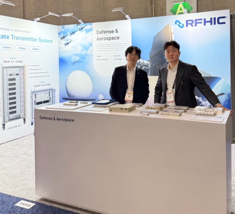
Alongside the MMIC lineup, RFHIC presented a full portfolio of field-proven GaN solutions:
Our GaN hybrid amplifiers for predrivers, designed for 5G and 6G applications, operating across sub-6 GHz bands and 50 Ω matched for fast, simplified integration. Our high-power GaN transistors for wireless infrastructure, and our turn-key GaN power amplifier solution — a compact, intelligent, time-saving module that pairs a pre-driver and main transistor with an evaluation board, all 50 Ω matched to shrink design cycles and footprint at once.
For defense and aerospace, we showcased our GaN solid-state power amplifiers (SSPAs) spanning L-band through Ku-band with kilowatt-class output
RFHIC GaN SSPA — High-Power Solid-State Power Amplifiers
| GaN-on-SiC solid-state amplifiers | 50 Ω input/output matched | Customized solutions available on request | ||||||||
| P/N | Band | Min Freq (MHz) | Max Freq (MHz) | Output Power (W) | Gain (dB) | VDC (V) | Efficiency (%) | Datasheet |
|---|---|---|---|---|---|---|---|---|
| RRP131K0-10 | L-band | 1200 | 1400 | 1000 | 53 | 50 | 45 | Datasheet |
| RRP27371K5-30 | S-band | 2700 | 3700 | 1500 | 30 | 50 | 35 | Datasheet |
| RRP54591K2-42 | C-band | 5400 | 5900 | 1200 | 40 | 50 | 25 | Datasheet |
| RRP54592K4-24 | C-band | 5400 | 5900 | 2400 | 24 | 50 | 25 | Datasheet |
| RRP5758065-40 | C-band | 5725 | 5850 | 65 | 40 | 32 | 35 | Datasheet |
| RRM9395200-56A | X-band | 9300 | 9500 | 200 | 56 | 50 | 25 | Datasheet |
| RRM9397800-59A | X-band | 9300 | 9700 | 800 | 59 | 50 | 20 | Datasheet |
| RRP099104080-49 | X-band | 9900 | 10400 | 80 | 49 | 40 | 25 | Datasheet |
| RRP162168100-08A | Ku-band | 16200 | 16800 | 100 | 8 | 50 | 20 | Datasheet |
our wideband amplifiers for electronic warfare and multi-function platforms, and our transmit & receive modules for advanced radar front ends.
RFHIC GaN Wideband Amplifiers
| GaN-on-SiC solid-state amplifiers | 50 Ω input/output matched | Customized solutions available on request | ||||||||
| P/N | Band | Min Freq (MHz) | Max Freq (MHz) | Output Power (W) | Gain (dB) | VDC (V) | Efficiency (%) | Datasheet |
|---|---|---|---|---|---|---|---|---|
| RWP03040-10 | Wideband | 20 | 520 | 40 | 40 | 28 | 53 | Datasheet |
| RWM0105050-47 | Wideband | 20 | 520 | 50 | 47 | 32 | 50 | Coming Soon |
| RWM0110050-47 | Wideband | 20 | 1000 | 50 | 47 | 32 | 50 | Coming Soon |
| RWP06040-6H | Wideband | 500 | 1000 | 40 | 42 | 28 | 50 | Coming Soon |
| RWP15080-10 | Wideband | 700 | 2500 | 100 | 53 | 32 | 35 | Datasheet |
| RWP1030050-37 | Wideband | 1000 | 3000 | 50 | 37 | 32 | 40 | Datasheet |
| RWP2540200-53 | Wideband | 2500 | 4000 | 200 | 50 | 48 | 34 | Datasheet |
| RWP5872050-10 | Wideband | 5800 | 7200 | 50 | 35 | 32 | 44.8 | Datasheet |
| RWP0427100-53 | Wideband | 400 | 2700 | 80 | 49 | 32 | 30 | Coming Soon |
| RWP2560050-10 | Wideband | 2500 | 6000 | 50 | 47 | 28 | 22 | Coming Soon |
| RWP05120-51 | Wideband | 20 | 1000 | 120 | 56 | 28 | 40 | Datasheet |
| RWP2060080-50 | Wideband | 2000 | 6000 | 80 | 50 | 36 | 22 | Datasheet |
| RWP4060100-50 | Wideband | 4000 | 6000 | 100 | 50 | 36 | 25 | Datasheet |
| RWP0409100-50 | Wideband | 395 | 930 | 80 | 49 | 28 | 45 | Coming Soon |
| RWP2040400-19 | Wideband | 2000 | 4000 | 400 | 19 | 50 | 25 | Datasheet |
Rounding out the display, our GaN solid-state microwave generators demonstrated how RFHIC’s technology scales from semiconductor processing and CVD to medical and industrial heating applications.
Each of these is summarized here only at a glance — the full specifications, performance data, and customization options are best explored in a direct conversation with our engineering team.
IMS 2026 wasn’t just a showcase; it was the start of new collaborations. Throughout the week, RFHIC met with customers, system integrators, and research partners from around the world to explore how our GaN technology can solve their toughest RF challenges — and to shape the roadmap for what comes next.
If you visited our booth, thank you. If you didn’t, it’s not too late. The portfolio we put on the floor in Boston is only the beginning of what RFHIC can do for your system — and many of our most powerful solutions are tailored to the specific demands of your application.
Curious how RFHIC’s GaN MMICs and amplifiers could elevate your next design? We’d love to show you.
Learn More (Click)
About RFHIC
RFHIC (KOSDAQ: A218410) is a global leader in GaN RF and microwave solutions, specializing in wireless communications, defense, aerospace, and industrial RF energy applications. The company develops and manufactures high-power GaN transistors, MMICs, solid-state power amplifiers, and microwave generator systems, all produced in-house for superior quality and performance. RFHIC is committed to advancing next-generation power semiconductor technologies to create a more connected, energy-efficient, and innovative future. Learn more at www.rfhic.com.
RFHIC® is a registered trademark.
Media Contact
Grace Cho
RFHIC Corporation
Head of Global Sales & Marketing
5G Wireless Infrastructure GaN: Why GaN-on-SiC is the Non-Negotiable Standard for 2026By 2026, the success of your massive MIMO deployment depends less on raw signal strength and more on how effectively you manage heat at the transistor level. While GaN-on-Silicon was once a viable entry point, the thermal demands of modern 5G wireless infrastructure GaN applications have rendered it obsolete for high-performance base stations. You’ve likely already faced the frustrations of thermal throttling in high-density arrays or the prohibitive weight of massive heat sinks required to keep sub-6GHz systems stable. These aren’t just engineering inconveniences; they’re fundamental barriers to scaling network capacity.
This article demonstrates why GaN-on-SiC has become the non-negotiable standard for engineers who need to maximize power-added efficiency and reduce unit weight. We’ll analyze the critical performance gap between Silicon Carbide and Silicon substrates, focusing on SiC’s superior thermal conductivity of up to 490 W/m·K compared to the mere 150 W/m·K offered by Si. You’ll discover how choosing the right substrate allows for a significant reduction in footprint while future-proofing your systems for the upcoming transition to 6G frequencies. We’ll provide a technical roadmap for optimizing SWaP-C through advanced GaN-on-SiC integration.
For decades, Laterally Diffused Metal Oxide Semiconductor (LDMOS) technology served as the undisputed workhorse of cellular base stations. It provided reliable, cost-effective performance for 3G and 4G LTE networks operating primarily at frequencies below 2.5 GHz. However, the architectural requirements of 5G have fundamentally altered the design landscape. Modern 5G wireless infrastructure GaN solutions have emerged as the only viable path forward as network operators push into higher spectrum bands to accommodate massive data throughput. Traditional silicon has reached its physical limits.
The global surge in 5G data traffic exerts immense pressure on Radio Access Network (RAN) power amplifiers. To maintain signal integrity across wider bandwidths, engineers have turned to High Electron Mobility Transistors (HEMT). These devices leverage the unique properties of Gallium nitride (GaN) to deliver high-speed switching and superior power density. Unlike LDMOS, which struggles with parasitic capacitance at higher frequencies, GaN HEMTs maintain high gain and efficiency even as the spectrum expands into the sub-6 GHz and millimeter-wave (mmWave) regions. This transition isn’t just an upgrade; it’s a necessity for survival in a high-capacity environment.
GaN is a wide bandgap (WBG) semiconductor, meaning it requires significantly more energy to move electrons from the valence band to the conduction band than silicon. This property results in a much higher breakdown voltage, allowing devices to operate at higher voltages without failure. Higher voltage operation directly correlates to increased power density, enabling smaller components to do the work of much larger silicon counterparts. The wide bandgap of GaN enables 5G systems to operate at significantly higher voltages and temperatures than silicon, effectively tripling the power density available for power amplification.
In the critical sub-6GHz bands, Power-Added Efficiency (PAE) is the metric that determines operational viability. LDMOS efficiency begins to degrade sharply as frequencies move past 3.5 GHz, leading to excessive heat generation. This creates a bottleneck for massive MIMO (mMIMO) arrays, which utilize 64T64R or 128T128R configurations. Packing dozens of inefficient silicon amplifiers into a single radio unit results in thermal loads that traditional cooling systems can’t manage. 5G wireless infrastructure GaN technology solves this by providing 10% to 20% higher PAE than LDMOS at these frequencies. This efficiency gain allows for smaller heat sinks and lighter overall units, which is essential for rooftop and pole-mounted installations where weight and size are strictly regulated.
While some manufacturers promote GaN-on-Silicon (GaN-on-Si) as a scalable, high-volume alternative, this approach often overlooks the critical thermal constraints of high-density networks. The strategic selection of substrates for 5G wireless infrastructure GaN systems determines the upper limit of network performance. Silicon Carbide (SiC) provides a superior foundation that manages the extreme heat generated by high-frequency power amplifiers. Choosing Si over SiC might reduce initial wafer costs, but it introduces significant thermal bottlenecks that compromise the entire system’s efficiency.
The core of the debate lies in thermal conductivity. Silicon Carbide exhibits a thermal conductivity of approximately 400 W/mK, whereas Silicon is limited to roughly 150 W/mK. This nearly 3x difference means that SiC-based devices can dissipate heat far more effectively than their Si-based counterparts. The widespread adoption of GaN semiconductors in 5G has validated this performance gap. When heat builds up at the transistor junction, it leads to power sagging and signal distortion. SiC’s ability to pull heat away from the active region keeps the device running cooler, which preserves signal linearity and extends the hardware’s operational life.
Thermal management isn’t just about cooling; it’s about reliability. High-heat environments accelerate degradation, directly impacting the Mean Time to Failure (MTTF) of base station components. By utilizing GaN-on-SiC, operators can reduce the size and complexity of cooling hardware, such as bulky heat sinks and active fans. This reduction is vital for urban deployments where space is at a premium. Engineers seeking to minimize thermal resistance often turn to specialized GaN on SiC transistors to maintain peak performance under heavy traffic loads.
Power density is measured in Watts per millimeter (W/mm) of gate periphery. GaN-on-SiC consistently delivers higher power density than GaN-on-Si, allowing for smaller transistor footprints without sacrificing output. This high-power density is critical for shrinking 5G base station dimensions and enabling the integration of more antenna elements in massive MIMO arrays. Optimizing 5G wireless infrastructure GaN designs requires a shift from component-level cost analysis to a Total Cost of Ownership (TCO) perspective. While Si wafers are cheaper, the system-level savings in electricity, cooling, and maintenance make SiC the more economical choice over the long term.
In 2026, the success of high-density network deployments hinges on optimizing SWaP-C: Size, Weight, Power, and Cost. As the massive MIMO market is projected to reach USD 8.4 billion this year, the pressure on hardware manufacturers to deliver more capacity in smaller packages has intensified. Transitioning to 64T64R and 128T128R antenna arrays requires an unprecedented concentration of power amplifiers within the Radio Unit (RU). Traditional silicon-based solutions cannot meet these requirements. They are simply too heavy and inefficient to stay within the strict weight limits of existing telecom towers. By contrast, 5G wireless infrastructure GaN technology provides the power density required to pack high-element arrays into compact, lightweight enclosures.
Integrating advanced materials for 5G like GaN-on-SiC directly addresses the physical bottlenecks of massive MIMO. It allows for a radical reduction in heat sink volume, which leads to a cascading series of benefits. Lighter units reduce the structural reinforcement costs for towers. Higher efficiency reduces the monthly utility bills for carriers. When every watt saved translates into lower OpEx, the economic argument for GaN-on-SiC becomes undeniable. This material efficiency is the primary reason why 5G is expected to be the fastest-growing segment with a CAGR of 23.94% through 2035.
Miniaturization is the core objective for modern deployments. By integrating GaN MMICs into front-end modules, manufacturers achieve a significant reduction in footprint. Recent industry developments have focused on integrated GaN package designs that specifically target the needs of 5G Radio Units. These designs improve cost efficiency while simultaneously reducing the physical load on tower infrastructure. High-efficiency 5G wireless infrastructure GaN components ensure that carriers don’t have to choose between network capacity and operational sustainability. This streamlined approach to hardware design is essential for the rapid rollout of urban small cells.
Maintaining signal purity across wide bandwidths is a complex engineering challenge. High-power GaN devices must exhibit excellent linearity to work effectively with Digital Pre-Distortion (DPD) algorithms. Without this linearity, signal distortion would bleed into adjacent channels and violate regulatory standards. RFHIC’s specialized GaN on SiC Transistors for wireless infrastructure provide a distinct advantage here. They offer the electron mobility and breakdown voltage necessary to handle wideband signals without compromising integrity. This ensures that even as bandwidth requirements grow toward the 6G era, the infrastructure remains stable, reliable, and compliant.
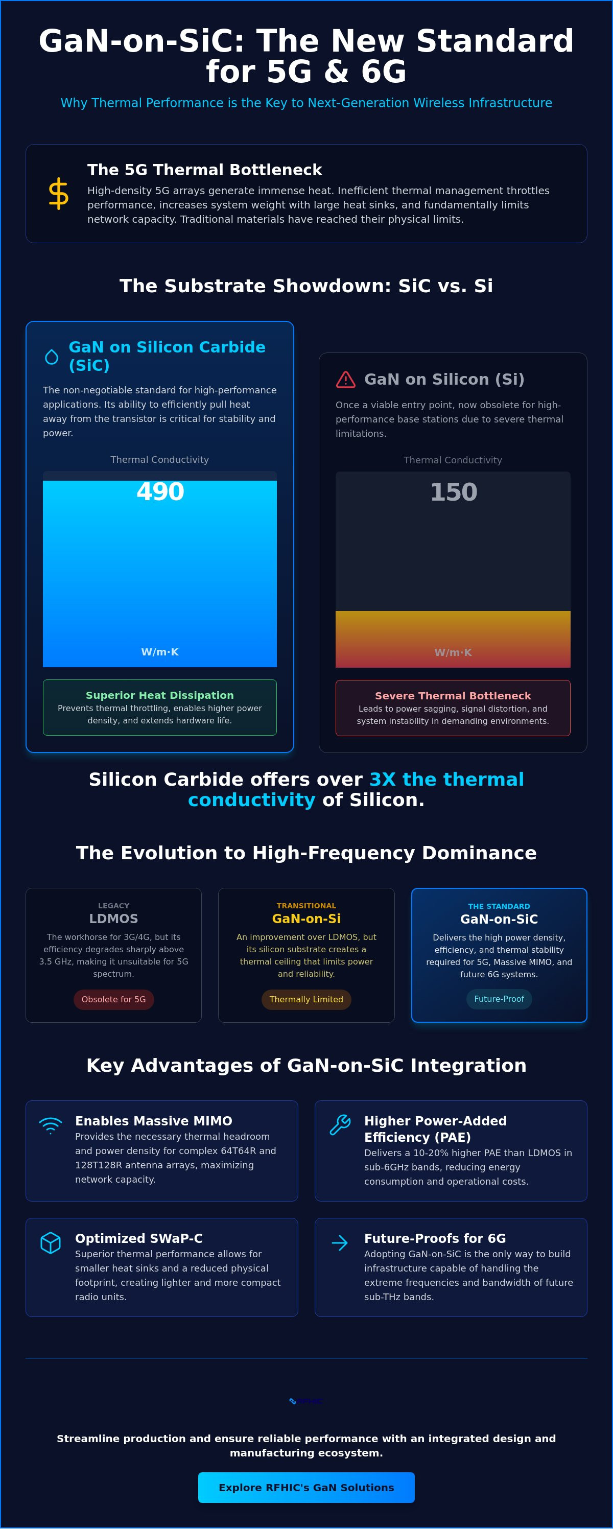
The roadmap toward 6G begins long before the first commercial networks go live in 2030. While 2026 represents the peak of 5G Advanced deployments, the engineering focus is already shifting toward the D-band (110-170 GHz) and sub-THz frequencies. These extreme spectral regions demand semiconductors with significantly higher electron mobility and power density than current standards. While existing 5G wireless infrastructure GaN solutions successfully navigate the sub-6 GHz and early mmWave bands, 6G introduces unprecedented path loss challenges. Overcoming these requires a material foundation that doesn’t just manage heat, but thrives under extreme power levels.
GaN-on-SiC remains the primary engine for this transition. It provides the necessary bandwidth and efficiency to sustain signal integrity at frequencies where silicon-based alternatives fail. For the most demanding ultra-high-power 6G applications, the industry is exploring GaN-on-Diamond. Diamond’s thermal conductivity is several times higher than even Silicon Carbide. This offers a potential path to manage the intense heat generated by sub-THz range extension. This evolution ensures that the infrastructure remains scalable and reliable as data demands continue to climb. By 2030, GaN will be the primary semiconductor enabling commercial 6G sub-THz links and intelligent, AI-managed radio access networks.
Moving beyond the 24 GHz ceiling requires extreme power at mmWave and sub-THz levels to compensate for atmospheric absorption. Path loss is the primary enemy of 6G. Engineers must deploy high-gain, high-power amplifiers to maintain link budgets over meaningful distances. RFHIC is currently evolving its technology to meet these sub-THz requirements, focusing on maximizing gain at the device level. This specialized hardware is essential for bridging the gap between current 5G capacity and the terabit-per-second goals of 6G. To prepare for these next-generation spectral demands, explore our high-performance GaN on SiC transistors for infrastructure applications.
6G base stations will utilize artificial intelligence to manage energy consumption dynamically. This requires power amplifiers that can switch states rapidly without losing efficiency. The synergy between GaN’s high switching speed and AI-managed beamforming allows networks to scale power output in real-time based on user traffic. This reduces wasted energy during low-traffic periods while maintaining peak performance during surges. 5G wireless infrastructure GaN technology provides the agility needed for these intelligent, self-optimizing networks. As AI becomes deeply integrated into the Radio Access Network (RAN), the rapid response times of GaN-on-SiC will be a critical enabler of network-wide power savings.
While previous sections established the thermal and efficiency advantages of the material, the practical implementation of 5G wireless infrastructure GaN requires a partner with end-to-end manufacturing control. RFHIC operates as a singular source of truth in the semiconductor landscape. We maintain total oversight from the initial transistor design to the final assembly of complete transmitter systems. This vertical integration eliminates the fragmentation often found in global supply chains. It ensures that every component meets the rigorous standards required for 2026 deployments. Our internal design and manufacturing capabilities allow for rapid prototyping and precise quality control. We don’t just provide parts. We deliver integrated solutions that solve the specific bottlenecks of modern Radio Access Networks. This mastery of the craft positions RFHIC as a dependable partner for OEMs who cannot afford the risks of multi-vendor dependencies.
The ecosystem begins with our high-performance GaN on SiC Transistors for Wireless Infrastructure. These discrete components provide the foundation for high-gain, high-efficiency amplification. However, we also provide GaN Solid-State Power Amplifiers (SSPAs) as complete, ready-to-integrate base station modules. This flexibility allows telecom OEMs to choose the level of integration that fits their specific architecture. By controlling the entire process, we ensure that the thermal management strategies discussed earlier are baked into the hardware at every level. Our internal control allows us to optimize the interface between the transistor and the heat sink, maximizing the 490 W/m·K thermal conductivity potential of the SiC substrate.
Every carrier operates on unique frequency bands and under specific environmental constraints. We offer comprehensive OEM Services to address these variations. Our engineering teams collaborate directly with clients to develop custom GaN solutions tailored to specialized 5G and future 6G requirements. This collaborative approach leverages our extensive experience in defense-telecom dual-use technology. The same reliability required for high-stakes radar systems is applied to commercial wireless infrastructure. This cross-industry expertise ensures that our hardware performs under the most demanding conditions. For manufacturers looking to secure their roadmap through 2030, the choice of a technology partner is critical. We provide the stability, innovation, and high-volume production capacity necessary to lead the market. Explore RFHIC’s GaN on SiC solutions for 5G and 6G to see how our integrated ecosystem can streamline your next deployment.
The transition from silicon-based legacy systems to high-performance GaN-on-SiC is no longer a matter of preference; it’s a structural requirement for 2026 and beyond. As established throughout this analysis, the superior thermal conductivity of Silicon Carbide is the only viable method for managing the extreme power densities of massive MIMO and sub-THz frequencies. By prioritizing SWaP-C optimization today, you’re building a foundation that can scale into the 6G era without the need for frequent hardware overhauls. High-efficiency 5G wireless infrastructure GaN solutions provide the reliability and performance density required to meet the world’s exponential data demands.
RFHIC brings over 20 years of GaN innovation to every partnership, serving as a trusted global supplier to Tier-1 telecom and defense OEMs. Our proprietary GaN on SiC technology ensures that your systems remain stable under the most demanding thermal loads while reducing overall unit weight. We invite you to leverage our end-to-end design and manufacturing ecosystem to streamline your deployment and maximize network capacity. Partner with RFHIC for your next-generation 5G GaN infrastructure and take control of your technical roadmap. The path to a faster, more efficient network starts with a commitment to superior semiconductor materials.
GaN-on-SiC is preferred because it offers significantly higher thermal conductivity, typically ranging from 330 to 490 W/m·K. This is nearly triple the performance of GaN-on-Silicon, which is limited to approximately 150 W/m·K. In high-power 5G environments, this superior heat dissipation allows for higher power density and prevents the thermal throttling that often degrades signal quality in silicon-based substrates.
GaN technology improves efficiency by delivering a higher Power-Added Efficiency (PAE) than traditional LDMOS. By converting a larger percentage of DC power into RF energy, GaN reduces the amount of power wasted as heat. This efficiency is vital for 5G wireless infrastructure GaN applications, as it directly lowers the electricity consumption of base stations and reduces the cooling requirements for dense network deployments.
In Massive MIMO arrays, GaN acts as the primary enabler for high-element configurations such as 64T64R and 128T128R. Its high power density allows engineers to pack dozens of power amplifiers into a compact radio unit. This miniaturization is essential for maintaining a manageable footprint while delivering the massive data throughput and beamforming capabilities required for urban 5G coverage.
Yes, GaN-on-SiC is uniquely suited for the sub-THz and D-band frequencies expected in the 6G era. The material’s high electron mobility and breakdown voltage allow it to maintain gain and efficiency at frequencies well above 100 GHz. This makes it a critical foundation for overcoming the extreme path loss challenges associated with the next generation of wireless communication.
GaN-on-SiC facilitates a significant reduction in both size and weight by minimizing the volume of cooling hardware. Because the material operates efficiently at higher temperatures and dissipates heat effectively, manufacturers can use smaller heat sinks. This weight reduction is critical for tower-mounted equipment, where structural load limits often restrict the installation of heavier, silicon-based radio units.
The primary advantage of a Silicon Carbide (SiC) substrate is its ability to pull heat away from the transistor junction with extreme efficiency. This prevents the formation of localized hot spots that can lead to device failure or performance degradation. By maintaining lower operating temperatures, SiC substrates ensure that the transistors achieve a longer Mean Time to Failure (MTTF) in demanding environments.
GaN-on-SiC is fully compatible with advanced Digital Pre-Distortion (DPD) techniques used to maintain signal linearity. Its predictable performance across wide bandwidths allows DPD algorithms to effectively correct for nonlinearities. This synergy is essential for 5G wireless infrastructure GaN systems to meet strict regulatory standards for signal purity and adjacent channel leakage ratios.
RFHIC supports telecom OEMs through an integrated ecosystem that includes discrete transistors, power amplifier modules, and complete transmitter systems. We offer specialized OEM Services to provide custom hardware tailored to specific frequency bands and power requirements. Our end-to-end control over the design and manufacturing process ensures supply chain reliability and technical excellence for high-volume infrastructure projects.
[News] RFHIC Advances Turquoise Hydrogen Production System Using GaN SSPA-Based Microwave Tech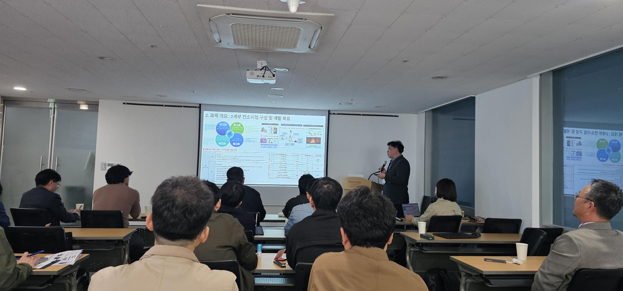
RFHIC is developing a core system for turquoise hydrogen production based on its GaN solid-state SSPA (Solid State Power Amplifier) microwave technology.
From April 21 to 23, a project performance review meeting was held in Jeju, Korea, under the support of the Korea Institute of Industrial Technology Evaluation and Planning (KEIT), affiliated with the Ministry of Trade, Industry and Energy.
The project, titled “Development of Turquoise Hydrogen Production and Continuous Carbon Material Manufacturing Using Underutilized Energy Resources,” brought together participating research institutions to review progress and discuss future development directions.
RFHIC is participating as the lead organization of Subproject 2, responsible for developing turquoise hydrogen production technology based on biogas.
Dr. Sangjin Kim, Head of Division at RFHIC, is responsible for the development of a continuous turquoise hydrogen production system utilizing GaN solid-state SSPA-based microwave technology.
Turquoise hydrogen is a hydrogen production method that enables the simultaneous generation of hydrogen and solid carbon without carbon dioxide emissions. In this project, a microwave heating-based process is applied to enable the conversion of underutilized biogas into hydrogen.
Key Technical Characteristics
Through this project, RFHIC is applying its GaN solid-state RF power amplifier and microwave technology to the clean hydrogen production sector.
This represents an expansion of RFHIC’s RF and microwave technologies, traditionally used in communications and defense, into the energy industry.
RFHIC is securing core equipment technologies for turquoise hydrogen production and plans to establish a new growth foundation in hydrogen production and continuous carbon material manufacturing.
The solid carbon generated during the turquoise hydrogen production process can be utilized as a carbon material.
As part of the project, research is also being conducted on the potential applications of this carbon material. Subproject 2 involves collaboration among RFHIC, the Korea Research Institute of Chemical Technology (KRICT), EST, and RIST, focusing on both hydrogen production systems and carbon material utilization technologies.
Reference: Read the original article
RFHIC is expanding its GaN solid-state RF and microwave technologies into clean hydrogen, carbon material manufacturing, and advanced energy applications.
Contact RFHIC to discuss technology collaboration, R&D opportunities, or microwave-based energy system applications.

RFHIC announced that it has signed a contract with the POSTECH Accelerator Laboratory to supply high-power solid-state power amplifiers (SSPA) for a multi-purpose synchrotron radiation accelerator project.
The contract is valued at approximately KRW 18.7 billion (USD equivalent) and will run from February 11, 2026 through December 31, 2029.
This project marks an important milestone for RFHIC as the company expands beyond its traditional telecommunications and defense RF semiconductor business into RF energy systems supporting national research infrastructure and advanced scientific facilities.
A synchrotron radiation accelerator is a large-scale research facility that accelerates electrons to near the speed of light to generate extremely bright and precise X-ray beams. These beams allow researchers to analyze the microscopic structure and dynamic behavior of materials with high precision.
Such facilities play a critical role in semiconductor research, advanced materials, biotechnology, energy technologies, and other cutting-edge scientific fields. The fourth-generation synchrotron accelerator involved in this project offers significantly improved brightness and precision, enabling more accurate analysis and real-time observation.
The RF amplification system to be supplied by RFHIC will incorporate high-power SSPAs based on the company’s proprietary Gallium Nitride (GaN) semiconductor technology. The system is designed to deliver high energy efficiency, digital control capability, and reliable long-term operation, which are essential for continuous operation in large-scale research environments.
? Media Contact:
? Learn More
About RFHIC
RFHIC (KOSDAQ: A218410) is a global leader in GaN RF and microwave solutions, specializing in wireless communications, defense, aerospace, and industrial RF energy applications. The company develops and manufactures high-power GaN transistors, solid-state power amplifiers, and microwave generator systems, all produced in-house for superior quality and performance. RFHIC is committed to advancing next-generation power semiconductor technologies to create a more connected, energy-efficient, and innovative future. Learn more at www.rfhic.com.
RFHIC® is a registered trademark.
RFHIC and Rohde & Schwarz Korea Forge a Strategic MOU for GaN Technology Development
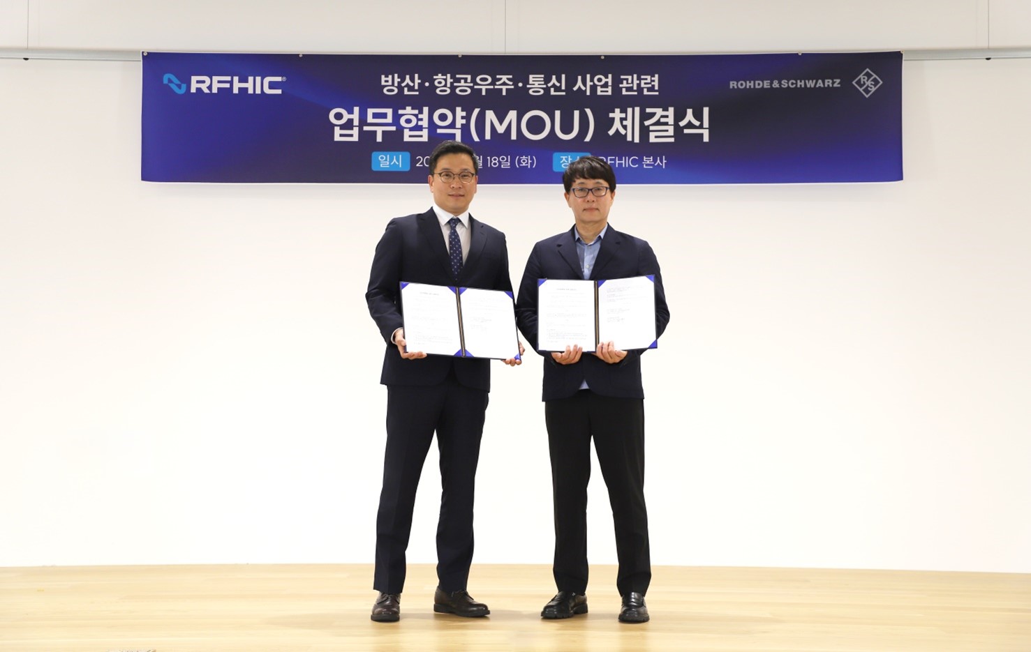
RFHIC and Rohde & Schwarz Korea Forge a Strategic MOU for GaN Technology Development
Gwacheon, South Korea, June 27th, 2024 – RFHIC Corporation (KOSDAQ:218410), a pioneer in the GaN RF & Microwave industry, have entered a strategic memorandum of understanding (MOU) focused on advancing gallium nitride (GaN) technology across defense, aerospace, and telecommunications sectors. This agreement marks a significant milestone that will combine the expertise and knowledge of both companies to foster innovation and extend their influence across various industries.
Under this MOU, Rohde & Schwarz Korea will provide RFHIC with state-of-the-art measurement solutions, including vector network analyzers, signal generators, spectrum analyzers, and oscilloscopes. These test & measurement instruments are expected to significantly enhance the verification processes in RFHIC’s GaN technology development and research initiatives.
Rohde & Schwarz Korea, the Korean subsidiary of Rohde & Schwarz that globally respected German company with a 90-year history, is renowned for delivering cutting-edge measurement solutions across telecommunications, broadcasting, electronics, and defense sectors. The company is recognized worldwide for its innovative technologies and quality products.
RFHIC, known for its pioneering role in high-power RF and microwave solid state power amplifiers (SSPA) utilizing GaN technology, collaborates closely in fields including defense, aerospace, and telecommunications. RFHIC’s SSPA products are widely utilized across these sectors, underlining the company’s leading position in the market.
Kim Tae-hoon, the Managing director of Rohde & Schwarz Korea, remarked, “This MOU between Rohde & Schwarz Korea and RFHIC will elevate Korea’s GaN technology development to a new level. The advanced measurement solutions of Rohde & Schwarz will play a pivotal role in RFHIC’s ongoing research and development efforts.”
RFHIC’s CEO, David Cho, also expressed optimism, stating, “Our collaboration with Rohde & Schwarz Korea will accelerate the development of GaN-based SSPA technology, significantly impacting the rapidly growing sectors of defense, aerospace, and telecommunications.”
Both companies are committed to maximizing their strengths through this collaboration, aiming to showcase further advanced technologies. For more details, visit the official websites and blog of Rohde & Schwarz Korea and RFHIC.
About RFHIC Corporation
RFHIC (KOSDAQ: A218410) is a global leader in designing and manufacturing GaN RF & Microwave components and systems for applications in wireless communications, defense and aerospace, and RF Energy (Industrial, Scientific, and Medical) segments. We provide industry-leading solutions for gallium-nitride (GaN) transistors, high-power solid-state power amplifiers, and high-power microwave generator systems, all within our in-house production facility. We enlighten industries with RF and Microwave advancements. To expedite a future enhanced by technological innovation – to create a better connected, safer, and stronger world for generations. Learn more at www.rfhic.com. RFHIC® is a registered trademark.
About Rohde & Schwarz
Rohde & Schwarz is striving for a safer and connected world with its Test & Measurement, Technology Systems and Networks & Cybersecurity Divisions. For 90 years, the global technology group has pushed technical boundaries with developments in cutting-edge technologies. The company’s leading-edge products and solutions empower industrial, regulatory and government customers to attain technological and digital sovereignty. The privately owned, Munich based company can act independently, long-term and sustainably. On June 30, 2023, Rohde & Schwarz had around 13,800 employees worldwide.
R&S® is a registered trademark of Rohde & Schwarz GmbH & Co. KG.
RFHIC Corporation
Grace Cho
Manager, Global Sales & Marketing
marketing@rfhic.com
Media Contacts
Rohde & Schwarz Korea
Jihong Choi
Manager, Marketing
Jihong.choi@rohde-schwarz.com
Gwacheon, South Korea, – April 15th, 2024 – RFHIC (KOSDAQ:A218410)

RFHIC Corporation, a pioneer in the GaN RF & Microwave industry, proudly announces a strategic investment in SweGaN AB, renowned for its cutting-edge development of Gallium Nitride on Silicon Carbide (GaN on SiC) epitaxial wafers, joins forces with RFHIC to usher in a new era of semiconductor excellence.
RFHIC has led the industry in creating and producing a diverse range of devices and high-powered subsystems based on GaN SiC technology. These products serve critical roles in various sectors, including 5g-advanced and 6g telecommunications, defense radar / electronic warfare, industrial applications, and beyond. Our strategic investment in SweGaN AB highlights our dedication to innovation and strengthens our supply chain. This move further enhances our position as a competitive leader in the RF and microwave markets.
We are confident that the combination of RFHIC’s technical expertise and resources with SweGaN’s QuanFINE® epitaxial technology positions us to accelerate the development of high-performance GaN semiconductors for a variety of high-power sectors. This strategic investment reflects our united vision of shaping the future with efficient and innovative semiconductor technologies.
In response to the surging demand for high-power, highly efficient semiconductors across a broad spectrum of applications — from 5g-advanced and 6g telecommunications and defense radars to high-power industrial uses — RFHIC is rapidly advancing its efforts. We are significantly expanding our internal research and development, enhancing our manufacturing capabilities, and diversifying our range of technological materials to meet and exceed market needs.
– Dr. Samuel Cho, CTO, and co-founder of RFHIC Corporation,
“As RFHIC maps its future strategy for GaN semiconductors including accelerated market demand for products in 5G-advanced, 6G, satellite communication and more, SweGaN’s high-performance 6-inch GaN epiwafers for RF and power semiconductors – with exemplary high-power efficiency – provide a strong fit for our technological roadmap and diversification of gallium nitride epitaxial wafer suppliers. SweGaN’s unique epitaxial wafer development and manufacturing technology is a key factor in the high performance of gallium nitride semiconductors that we can tap in developing new products in the 4GHz ultra-high frequency band increasingly sought after by the market.”
– Jr-Tai Chen, CEO and Founder at SweGaN,
“With the accelerating demand for high-performance semiconductor materials to power a multitude of applications and increase the efficiency in an energy-conscious world, the new equity investment will support SweGaN’s capacity expansion plan of its best-in-class GaN-on-SiC epitaxial wafers and tap joint product developments with RFHIC. We are very proud to partner with RFHIC, a leading RF GaN innovator who has the passion and commitment to amplify the world by providing top-efficiency and cutting-edge GaN solutions.”
In collaboration, RFHIC and SweGaN plan to address the increasing demand for GaN semiconductors and initiate new product developments for a variety of markets.
About RFHIC Corporation
RFHIC (KOSDAQ: A218410) is a global leader in designing and manufacturing GaN RF & Microwave components and systems for applications in wireless communications, defense and aerospace, and RF Energy (Industrial, Scientific, and Medical) segments. We provide industry-leading solutions for gallium-nitride (GaN) transistors, high-power solid-state power amplifiers, and high-power microwave generator systems, all within our in-house production facility. We enlighten industries with RF and Microwave advancements. To expedite a future enhanced by technological innovation – to create a better connected, safer, and stronger world for generations. Learn more at www.rfhic.com. RFHIC® is a registered trademark.
About SweGaN
SweGaN specializes in the development and production of engineered benchmark-performance Gallium Nitride on Silicon Carbide (GaN-on-SiC) epitaxial wafers, leveraging our innovative QuanFINE® growth technology. Our QuanFINE® material boasts exceptional performance, empowering our customers to swiftly address the dynamic challenges posed by next-generation high power and high-frequency devices, and to craft forward-looking solutions. We supply and offer tailored high-quality GaN epiwafers to the world’s leading foundries and manufacturers serving diverse sectors including satellite communications, telecommunications, defense sensing, and high-voltage power switches. For more information, visit us as www.swegan.se and LinkedIn.
RFHIC Corporation
Grace Cho
Manager, Global Sales & Marketing
Email: marketing@rfhic.com
SweGaN
Leslie Johnsen
Communications Advisor
Mob: +47 41 45 80 43
Email: leslie.johnsen@swegan.se
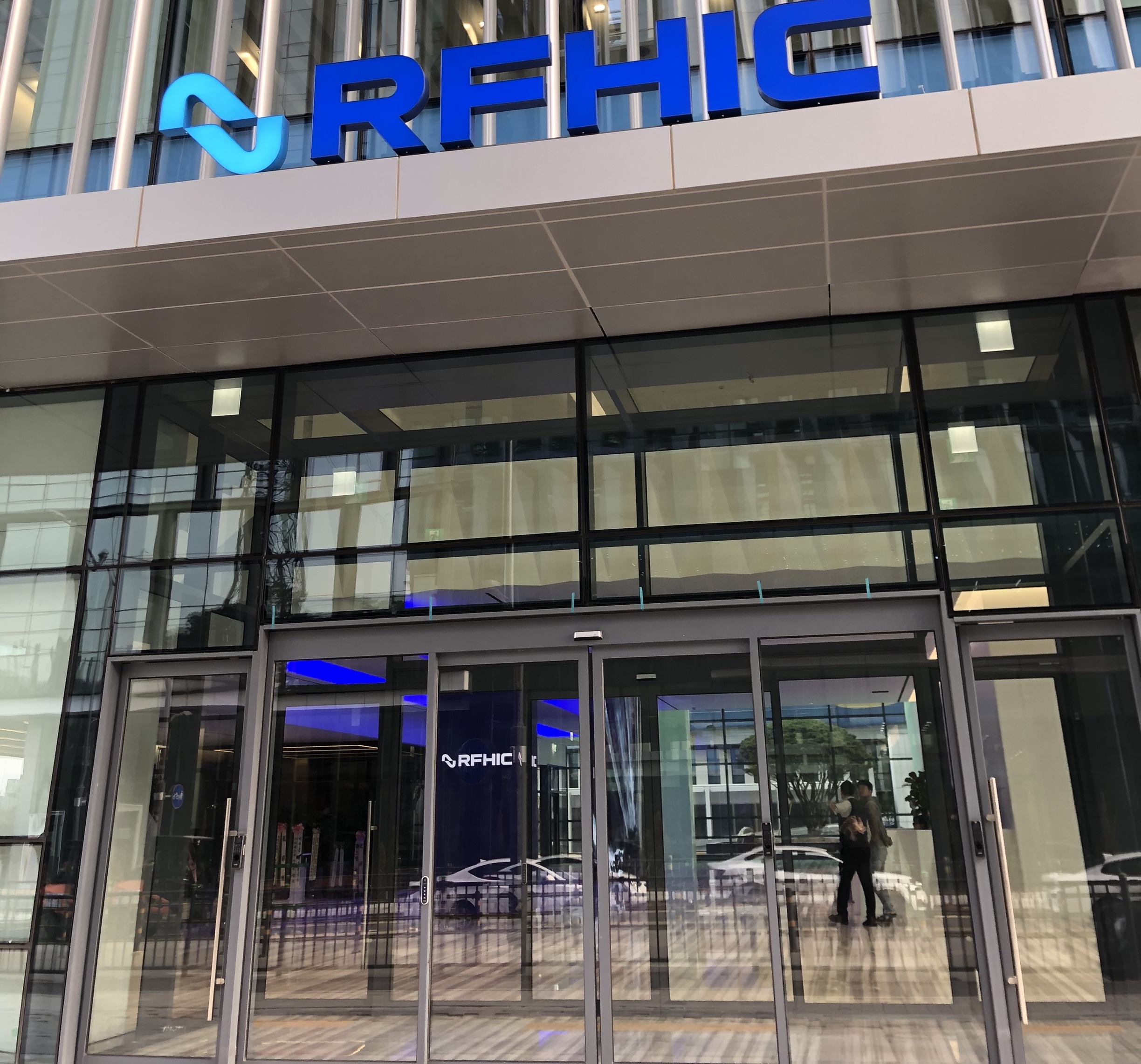
South Korea, Gwacheon – March 18th, 2024 – RFHIC (KOSDAQ: A218410)

We are excited to announce our new headquarters facility located in Gwacheon, South Korea!
Standing twelve stories tall, our new headquarters is located within the Gwacheon Knowledge Information Twon, which is Korea’s emerging hub for growing high-tech businesses.
The full address is RFHIC Bldg., 110 Gwacheon-daero 12-gil, Gwacheon-si, Gyeonggi-do, 13824, South Korea.
Our new headquarters will accomodate our expanding defense and RF energy business, while our previous HQ in Pyeongchon will continue to be used as a manufacturing facility.
Check out our new HQ below!


About RFHIC:
RFHIC (KOSDAQ: A218410) is a global leader in designing and manufacturing GaN RF & Microwave components and systems for applications in wireless communications, defense and aerospace, and RF Energy (Industrial, Scientific, and Medical) segments. We provide industry-leading solutions for gallium-nitride (GaN) transistors, high-power solid-state power amplifiers, and high-power microwave generator systems, all within our in-house production facility. We enlighten industries with RF and Microwave advancements. To expedite a future enhanced by technological innovation – to create a better connected, safer, and stronger world for generations. Learn more at www.rfhic.com.
RFHIC® is a registered trademark
Media Contact: